Pixel Design for Flexible Active Matrix Array

a flexible active matrix and pixel technology, applied in the direction of dielectric characteristics, instruments, radiation control devices, etc., can solve the problems of micro-cracks, delamination and other defects, degradation of film performance, and complete failure, so as to reduce stress/strain, reduce stress/strain, and reduce the effect of bending radius

Inactive Publication Date: 2016-03-03
SHARP KK
View PDF2 Cites 16 Cited by
  • Summary
  • Abstract
  • Description
  • Claims
  • Application Information

AI Technical Summary

Benefits of technology

[0008]Disclosed herein is a printed circuit board with conductive traces based on a serpentine design, to mitigate stress / strain to these lines when the underlying substrate is flexed. This design is considerably more robust against stress in any axis in which the substrate is flexed, as compared to straight lines, assuming that the period of the serpentine is short enough, so that the metal line is flat at each segment of this length, under the tightest radius of curvature expected. With respect to lines forming an array, the serpentine design of both the row and column lines (e.g., used to address a display or optical receiver) mitigates the stress under flexing.

Problems solved by technology

Many reliability problems have been associated with the use of flexible thin-film active-matrix arrays, when subjected to repetitive or extreme flexing.
It is well-known that when subjecting the materials that are used to make the array to high stress / strain, that micro-cracks, delamination, and other defects appear.
These defects result in the degradation of the film's performance, and eventually in its complete failure.
In particular, conductive, brittle layers are especially prone to this problem.
Even softer materials, such as aluminum, will exhibit degradation in their conductivity under repetitive flexing, before failure in the form of electrical opens.
This problem is currently addressed by (a) confining the flexible array in a suitable enclosure, which allows limited flexing, so that extreme bending radius is not allowed, and flexing is confined to certain axes or directions of the array plane, or (b) laminating protective layers at the top / bottom to mitigate stresses in the active plane, which also limits flexibility.
When tensile stress is applied in the X-axis (FIG. 2B), this design is shown to suffer from crack formation in the metal film length, resulting in degraded conductivity, and eventually open-circuit (breakage) failure.

Method used


Image

  • Pixel Design for Flexible Active Matrix Array
  • Pixel Design for Flexible Active Matrix Array
  • Pixel Design for Flexible Active Matrix Array

Examples


Embodiment Construction

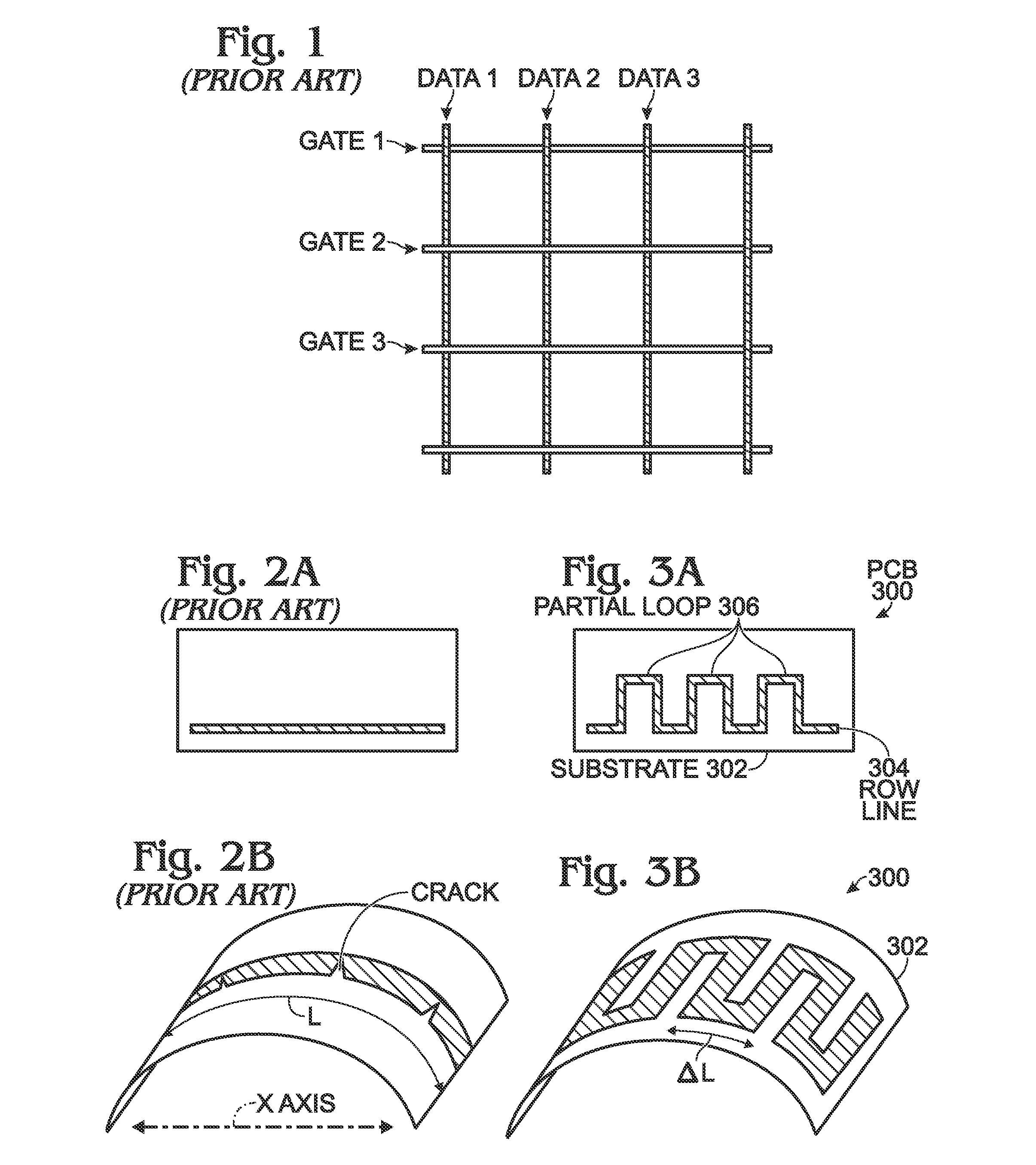
[0020]FIGS. 3A and 3B are views of a flexible printed circuit board (PCB). The PCB 300 comprises a flexible substrate 302 and a row line 304 overlying the substrate 302, formed in serpentine pattern with a plurality of partial-loops 306. As shown in FIG. 3B, the short length of the partial-loops components (ΔL) mitigate against the formation of cracks when the substrate 302 is flexed, in contrast to the PCB of FIG. 2B.

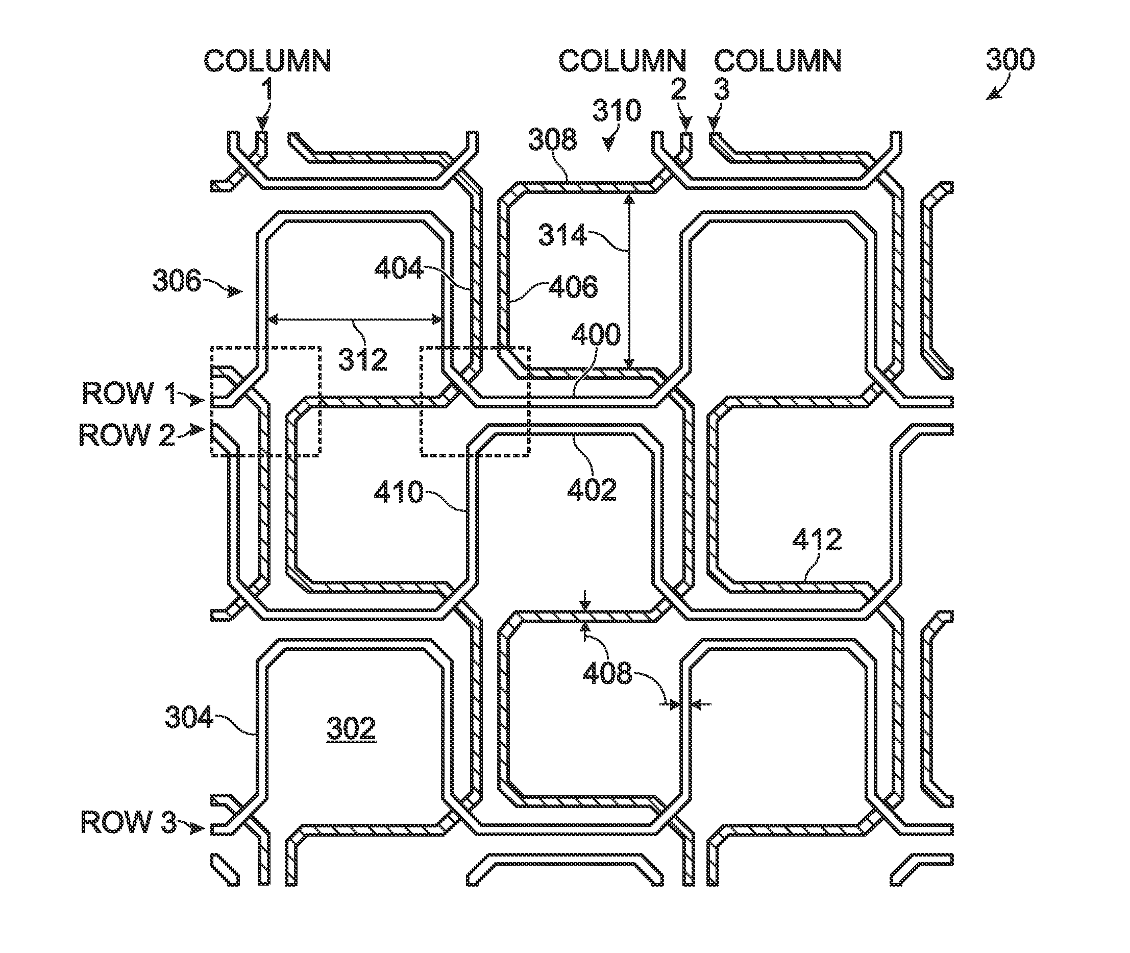
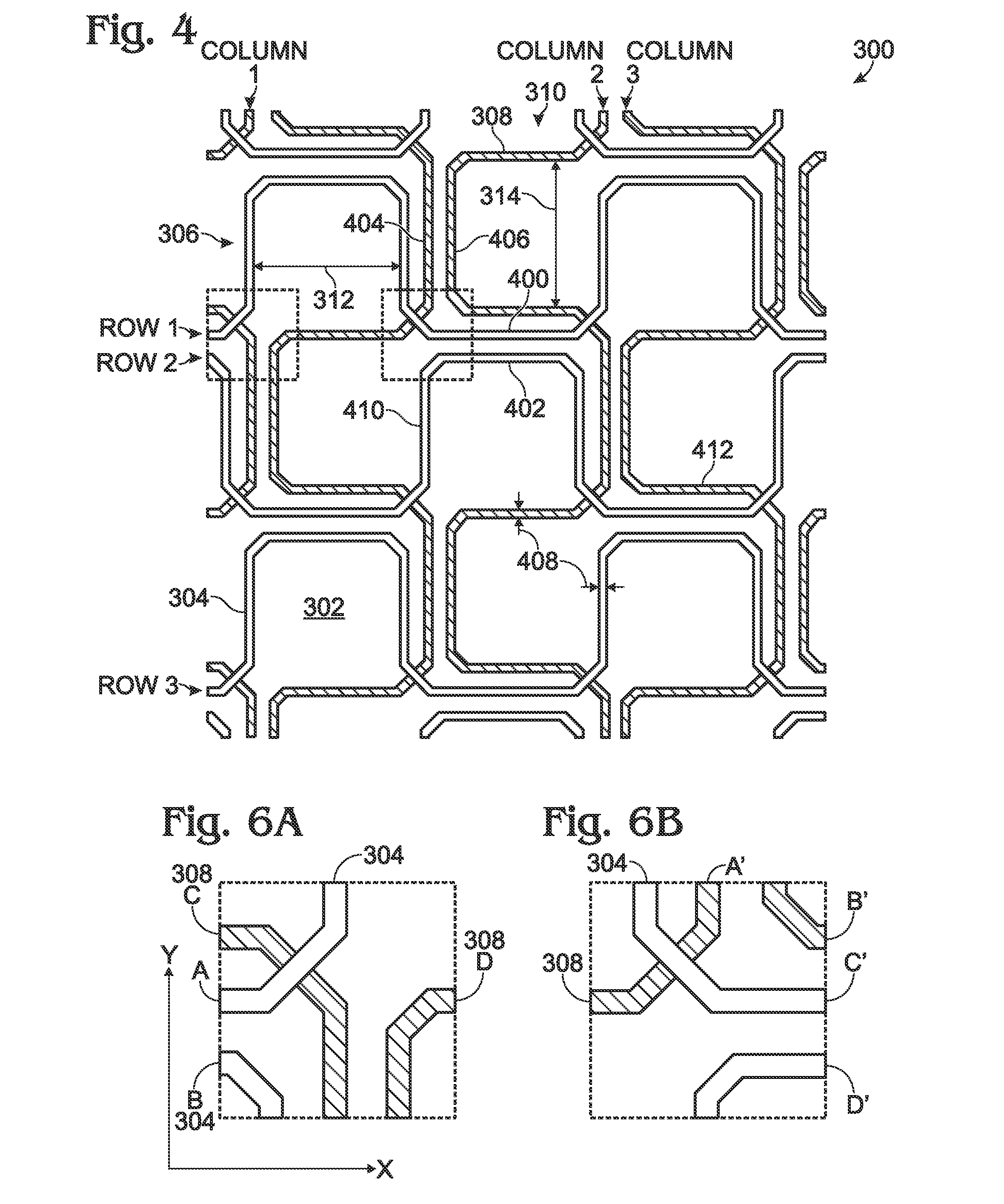
[0021]FIG. 4 is a plan view of a variation of the PCB of FIG. 3A. In this aspect, a plurality of parallel row lines 304 overlies the substrate 302. Each row line is formed in serpentine pattern with a plurality of partial-loops 306. A plurality of parallel column lines 308 overlies the substrate 302, orthogonal to the row lines 304. Each column line 308 is formed in a serpentine pattern with a plurality of partial-loops 310. A 3×3 pattern is shown, but the PCB is not necessarily so limited. As shown, the row line partial-loops 306 have a 3-sided rectangular shape with ...


PUM

PropertyMeasurementUnit
thicknessaaaaaaaaaa
widthaaaaaaaaaa
lengthaaaaaaaaaa

Abstract

A flexible active matrix array is provided, made with a flexible substrate and an array of pixels overlying the substrate, where each pixel includes an active device and a light controlling device. The array also includes a plurality of parallel row lines overlying the substrate, with each row line formed in serpentine pattern with a plurality of partial-loops, to supply a first signal to a corresponding plurality of pixels. A plurality of parallel column lines overlies the substrate, orthogonal to the row lines. Each column line is formed in a serpentine pattern with a plurality of partial-loops, to supply a second signal to a corresponding plurality of pixels. Each pixel has a border, with each row line partial-loop formed along about 75% of a pixel border, and each column line partial-loop formed along about 75% of a pixel border. Also provided is a printed circuit board with serpentine traces.

Description

BACKGROUND OF THE INVENTION[0001]1. Field of the Invention[0002]This invention generally relates to printed circuit board (PCB) design and, more particularly, to a PCB design permitting substrate flexibility, such as might be useful with a flexible electronic array.[0003]2. Description of the Related Art[0004]Many reliability problems have been associated with the use of flexible thin-film active-matrix arrays, when subjected to repetitive or extreme flexing. It is well-known that when subjecting the materials that are used to make the array to high stress / strain, that micro-cracks, delamination, and other defects appear. These defects result in the degradation of the film's performance, and eventually in its complete failure. In particular, conductive, brittle layers are especially prone to this problem. Even softer materials, such as aluminum, will exhibit degradation in their conductivity under repetitive flexing, before failure in the form of electrical opens. This problem is cu...

Claims


Application Information

Patent Timeline
Patent Type & Authority Applications(United States)
IPC IPC(8): H05K1/02G02F1/1333G02F1/1343G02F1/1368H01L27/12H01L27/146H01L27/15H01L27/32H01L51/00
CPCH05K1/028H05K1/0296G02F1/1368G02F1/133305G02F1/134336H01L2251/5338H01L27/1218H01L27/14612H01L27/15H01L27/3244H01L51/0097H01L27/124H05K1/0281H05K1/189H05K2201/0108H05K2201/09263H05K2201/10106H05K2201/10128H05K2201/10136Y02E10/549H10K59/131H10K77/111H10K2102/311H10K59/12
Inventor AFENTAKIS, THEMISTOKLES
Owner SHARP KK
Why Eureka
Try Eureka