Pattern analysis method of a semiconductor device

Active Publication Date: 2016-03-10
SAMSUNG ELECTRONICS CO LTD
View PDF14 Cites 15 Cited by
  • Summary
  • Abstract
  • Description
  • Claims
  • Application Information

AI Technical Summary

Benefits of technology

The patent describes a method for analyzing semiconductor device patterns and identifying areas of failure. The method involves extracting a contour image of the patterns, calculating a difference between the contour image and a target layout image, scoring the patterns based on the difference, and automatically identifying hotspots that indicate areas of failure. The method can also include reviewing the patterns, identifying the hotspots, and performing optical proximity correction after identifying the hotspots. The technical effect of this method is to improve the accuracy and efficiency of identifying areas of failure in semiconductor device patterns.

Problems solved by technology

However, various failure factors may be generated during the photo-etching process.

Method used


Image

  • Pattern analysis method of a semiconductor device
  • Pattern analysis method of a semiconductor device
  • Pattern analysis method of a semiconductor device

Examples


Embodiment Construction

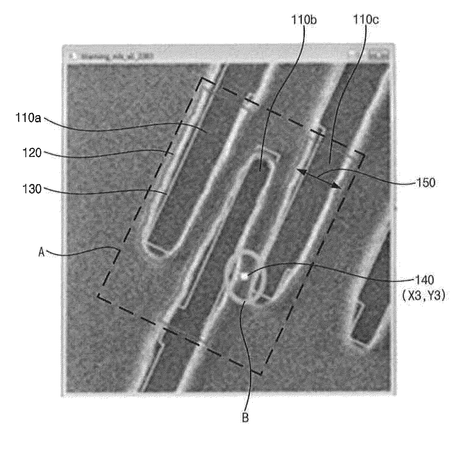
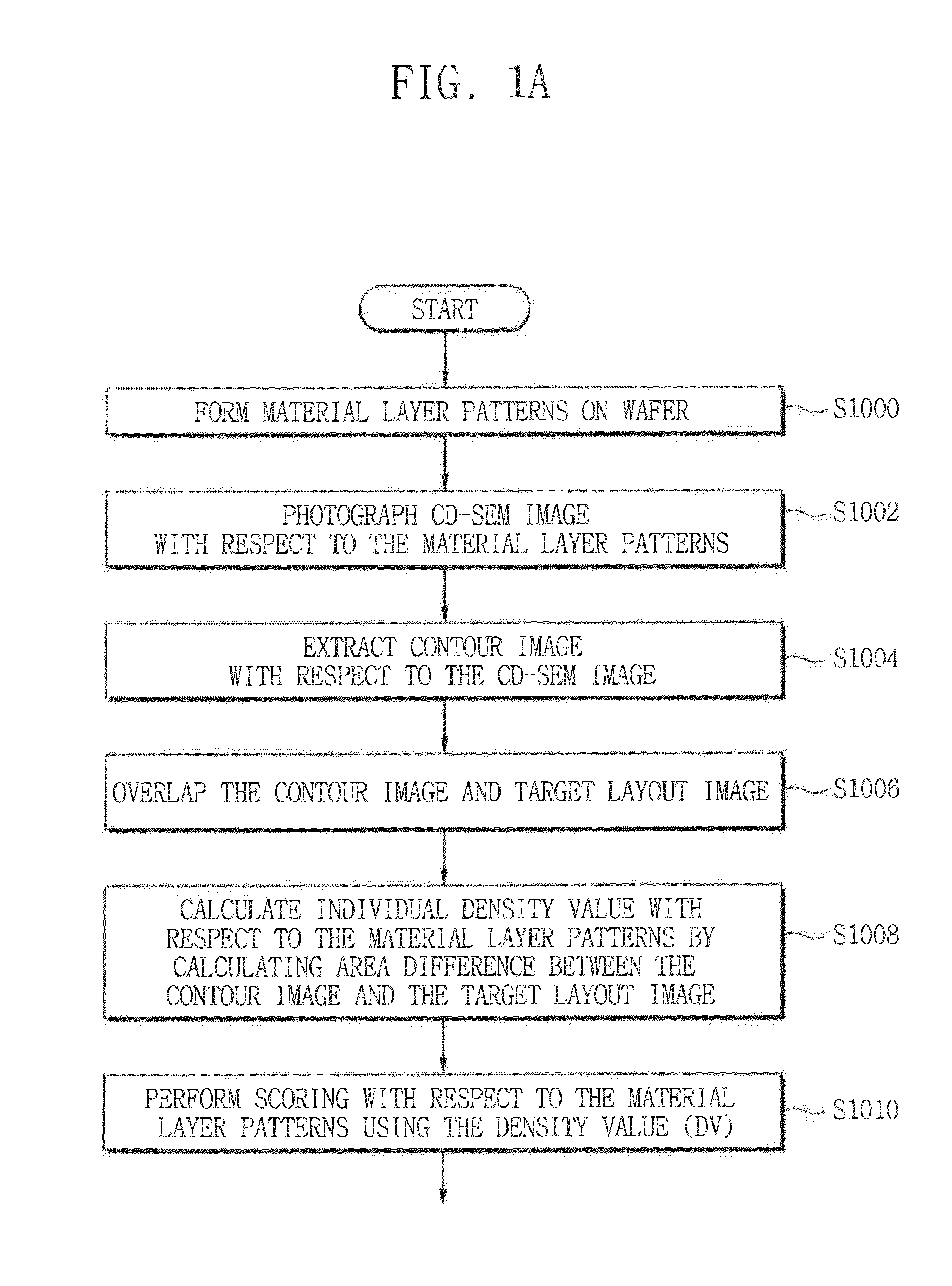
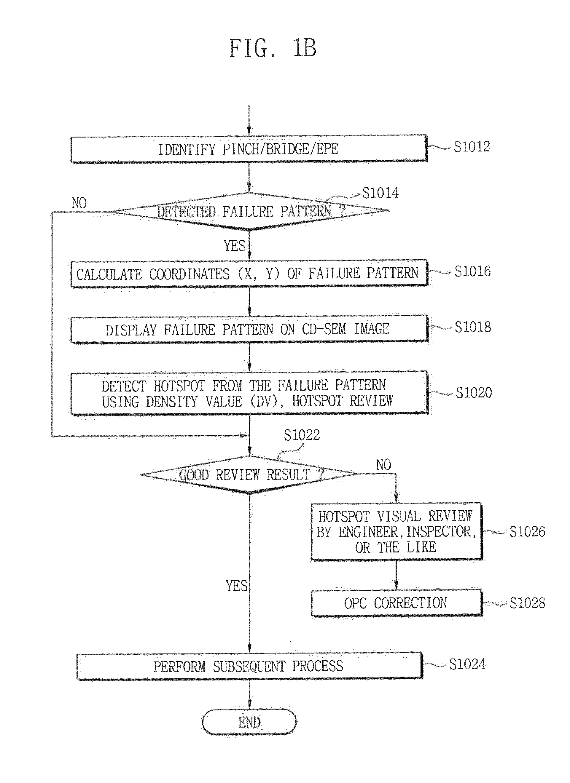
[0037]Exemplary embodiments of the inventive concept will now be described more fully with reference to the accompanying drawings. The invention may, however, be embodied in many different forms and should not be construed as being limited to the exemplary embodiments set forth herein.

[0038]As used herein, the singular forms “a,”“an,” and “the,” are intended to include the plural forms as well, unless the context clearly indicates otherwise.

[0039]Exemplary embodiments are described herein with reference to cross-sectional illustrations that are schematic illustrations of idealized embodiments (and intermediate structures). As such, variations from the shapes of the illustrations as a result, for example, of manufacturing techniques and / or tolerances, may be expected. For example, the exemplary embodiments should not be construed as limited to the particular shapes of regions illustrated herein but may include deviations in shapes that result, for example, from manufacturing. For exa...


PUM


Abstract

A pattern analysis method of a semiconductor device includes extracting a contour image of material layer patterns formed on a wafer, calculating an individual density value (DV) representing an area difference between the contour image and a target layout image, scoring the material layer patterns on the wafer using the individual DV, identifying a failure pattern among the scored material layer patterns, calculating coordinates of the identified failure pattern and displaying the coordinates on a critical dimension-scanning electron microscopy (CD-SEM) image, inputting a reference DV in the computer and automatically sorting the material layer patterns into material layer patterns having a hotspot and material layer patterns not having a hotspot, and reviewing the sorted material layer patterns having the hotspot.

Description

CROSS-REFERENCE TO RELATED APPLICATION[0001]This application claims priority under 35 U.S.C. §119 to Korean Patent Application No. 10-2014-0118917 filed on Sep. 5, 2014, the disclosure of which is incorporated by reference herein in its entirety.TECHNICAL FIELD[0002]Exemplary embodiments of the inventive concept relate to a pattern analysis method which detects failure factors (e.g., hotspots) on a wafer.DISCUSSION OF THE RELATED ART[0003]Patterns (or, structures) of various conductive or insulating layers of a semiconductor device are integrated on a wafer through a photo-etching process. The photo-etching process may include patterning a mask, exposing a layer, and developing the layer. However, various failure factors may be generated during the photo-etching process. These various failure factors may include the formation of a bridge, in which adjacent patterns on the wafer are undesirably connected, a pinch, in which a pattern has a width equal to or smaller than a critical dim...

Claims


Application Information

Patent Timeline
IPC IPC(8): G06T7/00G01N23/20H01J37/26H01L21/66
CPCG06T7/0008H01L22/12H01J37/26G06T2207/30148G06T7/001G06T2207/10061G06T2207/20076G01N23/20H01J37/222H01J37/28H01J2237/24592H01J2237/2816H01J2237/2817G01N23/2251
Inventor YANG, KIHOCHI, KAIYUANYANG, SEUNGHUNECAI, SIBO
Owner SAMSUNG ELECTRONICS CO LTD
Why Eureka
Try Eureka