Catalyst-induced growth of carbon nanotubes on tips of cantilevers and nanowires

a carbon nanotube and nanowire technology, applied in the direction of surface reaction electrolytic coating, chemical vapor deposition coating, cell, etc., can solve the problems of difficult adjustment of the length of the nanotube tip, poor electrical properties of carbon nanofibers, and high mechanical strength of nanotubes, so as to enhance the adhesion of the catalyst dot to the substrate and enhance the adhesion of the ni to the substrate

Inactive Publication Date: 2004-06-29
UT BATTELLE LLC +1
View PDF2 Cites 91 Cited by
  • Summary
  • Abstract
  • Description
  • Claims
  • Application Information

AI Technical Summary

Benefits of technology

The present invention can be used for production of carbon nanostructure-anchored cantilevers that can significantly improve the performance (such as resolution) of conventional scanning probe microscopy, for example, atomic force microscopy (AFM), scanning tunneling microscopy (STM), etc. The present invention can be used also in many other processes of micro and / or nanofabrication with carbon nanostructures.
Deposition of the catalyst dot 33 is preferably achieved by application of the above-described earlier invention in conjunction with the use of a liquid AFM system. As illustrated in FIG. 5, a solution of at least one metal catalyst compound, for example, NiCl.sub.2, CoCl.sub.2, Fe.sup.2+, etc., that are suitable for electrolytic deposition of the desired catalyst is added into a liquid AFM cell 39. With the liquid AFM system, the tip 45 of a conductive AFM cantilever 31 can be aligned with the tip 47 of a nanowire or another cantilever 43 pointing up. The cathodic tip 45 to anodic tip 47 spacing can easily be controlled. Spacing of the tips 45, 47 should be regulated to ensure deposition of a metal catalyst dot 33 at the desired cathode location, because the electric field (E) is a vector that is strongly dependent on distance (r):

Problems solved by technology

Thirdly, carbon nanotubes exhibit high mechanical strength and flexibility and therefore will not break easily upon crashing into a sample surface, which is a fairly common accident in SPM.
One consequence of these defects is that the electrical properties of carbon nanofibers are not as good as for carbon nanotubes.
However, these procedures have a number of disadvantages: (a) the carbon nanotubes first must be grown at high temperatures and separated, cleaned and cut to length; (b) in most cases it is difficult to adjust the length of the nanotube tip and to obtain a strong, reliable attachment; and (c) these complicated manipulations of carbon nanotubes are impractical in an industrial environment or for large-scale production.

Method used


Image

  • Catalyst-induced growth of carbon nanotubes on tips of cantilevers and nanowires
  • Catalyst-induced growth of carbon nanotubes on tips of cantilevers and nanowires
  • Catalyst-induced growth of carbon nanotubes on tips of cantilevers and nanowires

Examples


example ii

Arrays of single carbon nanostructures were successfully grown directly on commercial SiN contact-mode AFM cantilevers utilizing the two-step process described above.

Carbon Nanostructure Growth on Flattened Tips

As described above, the catalyst dot 33 can be deposited onto very sharp tip 45, which is preferably pointing directly downward, as shown in FIG. 4, to achieve downward carbon nanostructure growth. Upward carbon nanostructure growth is best achieved with a slightly different technique, using a flat tip 83, as shown in FIGS. 8a, 8b. If a sharp tip 45 is inverted (with the tip pointing upwardly) during the heating process for nanostructure growth, the catalyst dot 33 may have a tendency slide down the side of the cantilever 31, resulting in carbon nanostructure growth in a lateral direction. Even slight displacement of the dot 33 can produce undesirable results. As shown in FIGS. 8a, 8b, a catalyst dot 33 on a flat tip 83 is unlikely to slide down the side of an inverted cantil...


PUM

PropertyMeasurementUnit
diametersaaaaaaaaaa
temperaturesaaaaaaaaaa
diameteraaaaaaaaaa

Abstract

A method is described for catalyst-induced growth of carbon nanotubes, nanofibers, and other nanostructures on the tips of nanowires, cantilevers, conductive micro / nanometer structures, wafers and the like. The method can be used for production of carbon nanotube-anchored cantilevers that can significantly improve the performance of scaning probe microscopy (AFM, EFM etc). The invention can also be used in many other processes of micro and / or nanofabrication with carbon nanotubes / fibers. Key elements of this invention include: (1) Proper selection of a metal catalyst and programmable pulsed electrolytic deposition of the desired specific catalyst precisely at the tip of a substrate, (2) Catalyst-induced growth of carbon nanotubes / fibers at the catalyst-deposited tips, (3) Control of carbon nanotube / fiber growth pattern by manipulation of tip shape and growth conditions, and (4) Automation for mass production.

Description

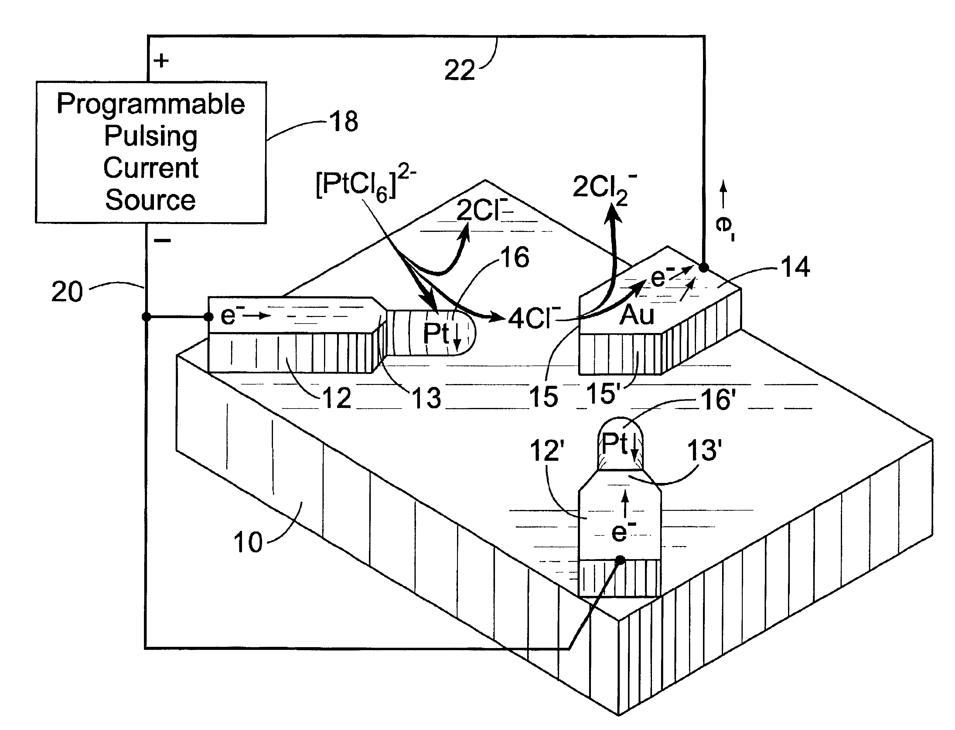
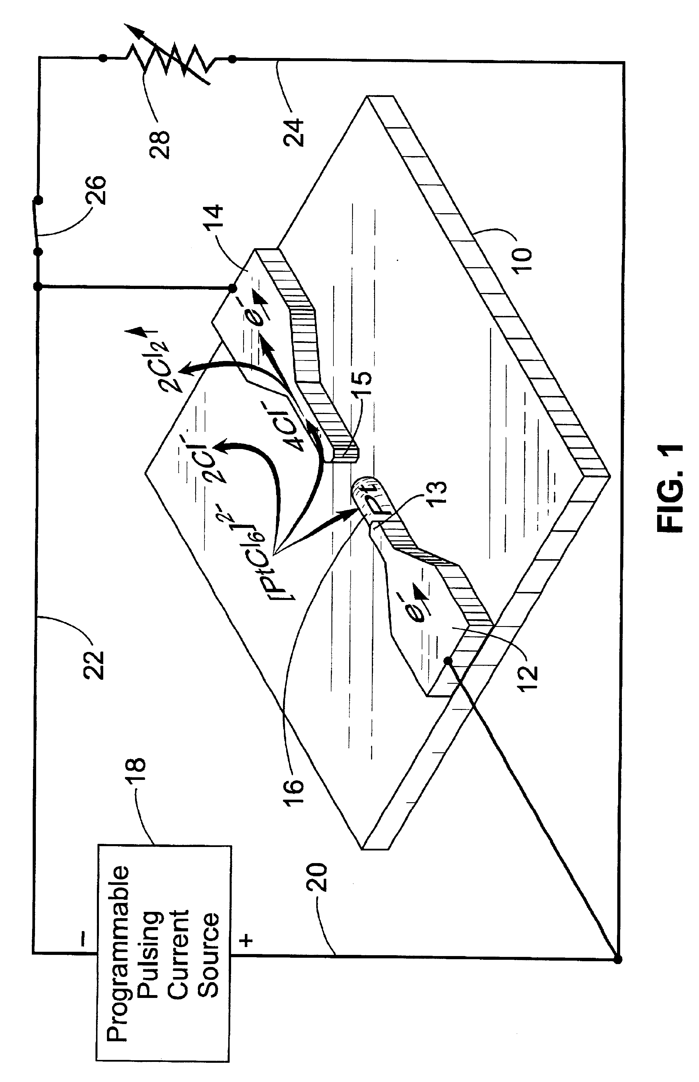
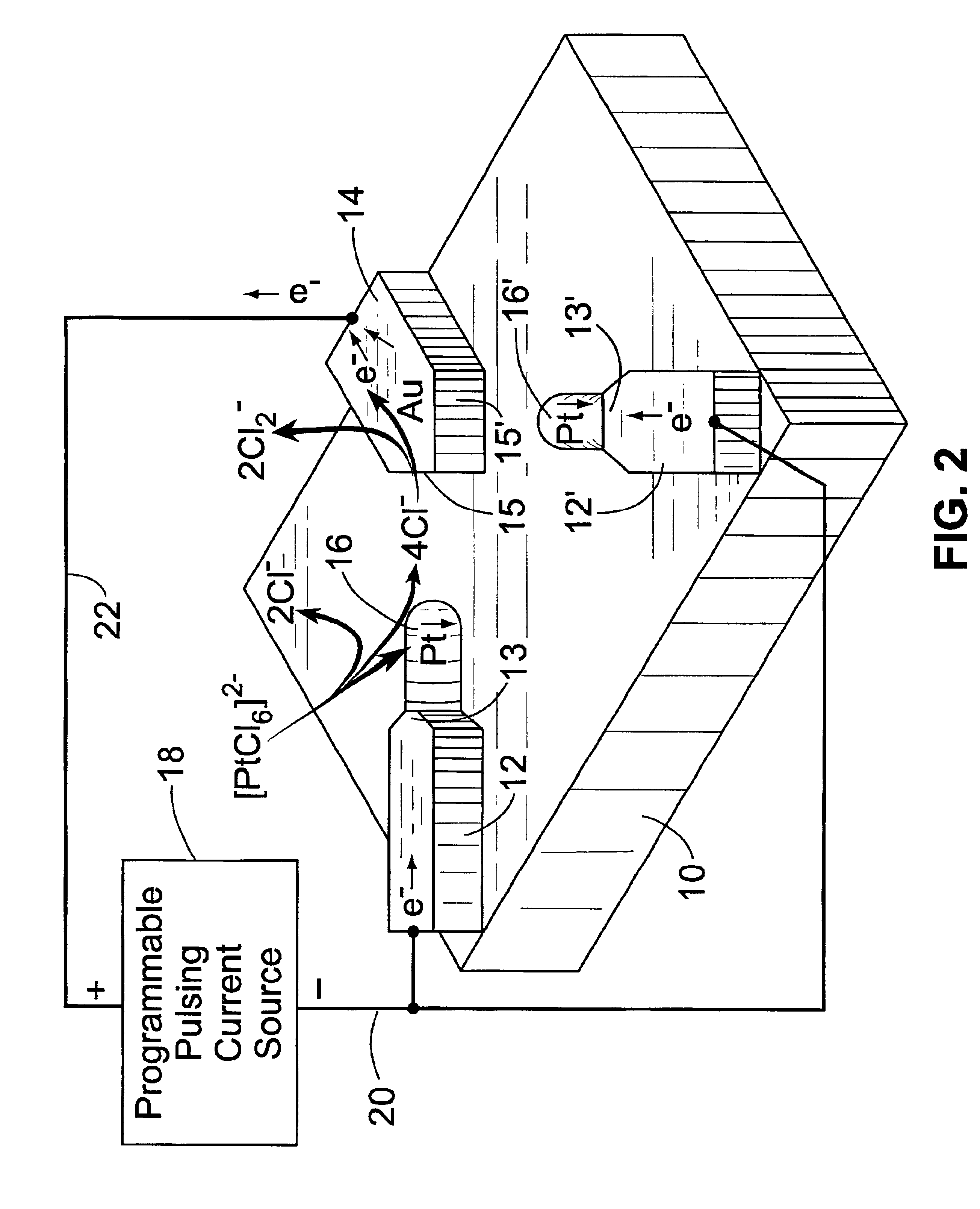
The present invention relates to carbon nanostructures and methods of growing the same, and more particularly to carbon nanostructures that are attached to catalyst dots, and catalyst-induced methods of growing carbon nanostructures, especially on the tips of cantilevers, nanowires, wafers, conductive micro / nanostructures, and the like.Programmable Nanometer-Scale Electrolytic Metal Deposition and DepletionA previous invention, referenced hereinabove, describes nanometer-scale deposition and / or depletion of nanostructures in liquids at preferably ambient temperature and preferably neutral pH through electric field-directed, programmable, pulsed electrolytic metal deposition or depletion.Application of a programmable and short (ns--ms time scale) pulsing direct current source is used to control the number of atoms being deposited by the electrolytic metal reduction and deposition process. As shown in the following platinum deposition reaction at a cathode using water-soluble hexachlo...

Claims


Application Information

Patent Timeline
Patent Type & Authority Patents(United States)
IPC IPC(8): C01B31/00C01B31/02C25D21/12C25D1/02C25D1/00C25D7/00C25D5/18C25D5/00G12B21/00G12B21/02B82B1/00B82B3/00G01Q70/16
CPCB82Y15/00B82Y30/00B82Y35/00B82Y40/00C01B31/0233C01B31/0293C25D1/02C25D5/18C25D7/00C25D21/12G01Q70/12C25D7/0607C01B2202/02C01B2202/06Y10S977/762Y10S977/843Y10S977/873Y10S977/876C01B32/162C01B32/18Y10T428/31504
Inventor LEE, JAMES WEIFULOWNDES, DOUGLAS H.MERKULOV, VLADIMIR I.ERES, GYULAWEI, YAYIGREENBAUM, ELIASLEE, IDA
Owner UT BATTELLE LLC
Why Eureka
Try Eureka