Organic light emitting display panel and method of manufacturing the same

a technology of light-emitting display panel and organic material, which is applied in the direction of basic electric elements, electrical apparatus, semiconductor devices, etc., can solve the problem of reducing the opening ratio of pixel area, and achieve the effect of reducing the area of the storage capacitor, and reducing the area of the capacitor

Active Publication Date: 2016-03-10
LG DISPLAY CO LTD
View PDF0 Cites 10 Cited by
  • Summary
  • Abstract
  • Description
  • Claims
  • Application Information

AI Technical Summary

Benefits of technology

[0007]An aspect of the present invention is to provide an organic light emitting display panel and a method of manufacturing the same, which can maintain or increase a capacitance while reducing the size of a capacitor by arranging the capacitors in parallel.
[0010]As described above, according to one or more embodiments of the present invention, storage capacitors are provided in parallel, therefore a capacitance of the storage capacitor can be maintained and the area of the storage capacitor can be reduced.
[0011]According to one or more embodiments of the present invention, two storage capacitors are formed in parallel using source / drain electrodes, and thus the area of a capacitor can be reduced.
[0012]According to one or more embodiments of the present invention, the area of the capacitor is reduced and a non-emissive area in a pixel area is reduced, thereby increasing an opening ratio.

Problems solved by technology

The larger the size of a capacitor is, the larger the capacitance is, but this may reduce an opening ratio of a pixel area.

Method used


Image

  • Organic light emitting display panel and method of manufacturing the same
  • Organic light emitting display panel and method of manufacturing the same
  • Organic light emitting display panel and method of manufacturing the same

Examples


Embodiment Construction

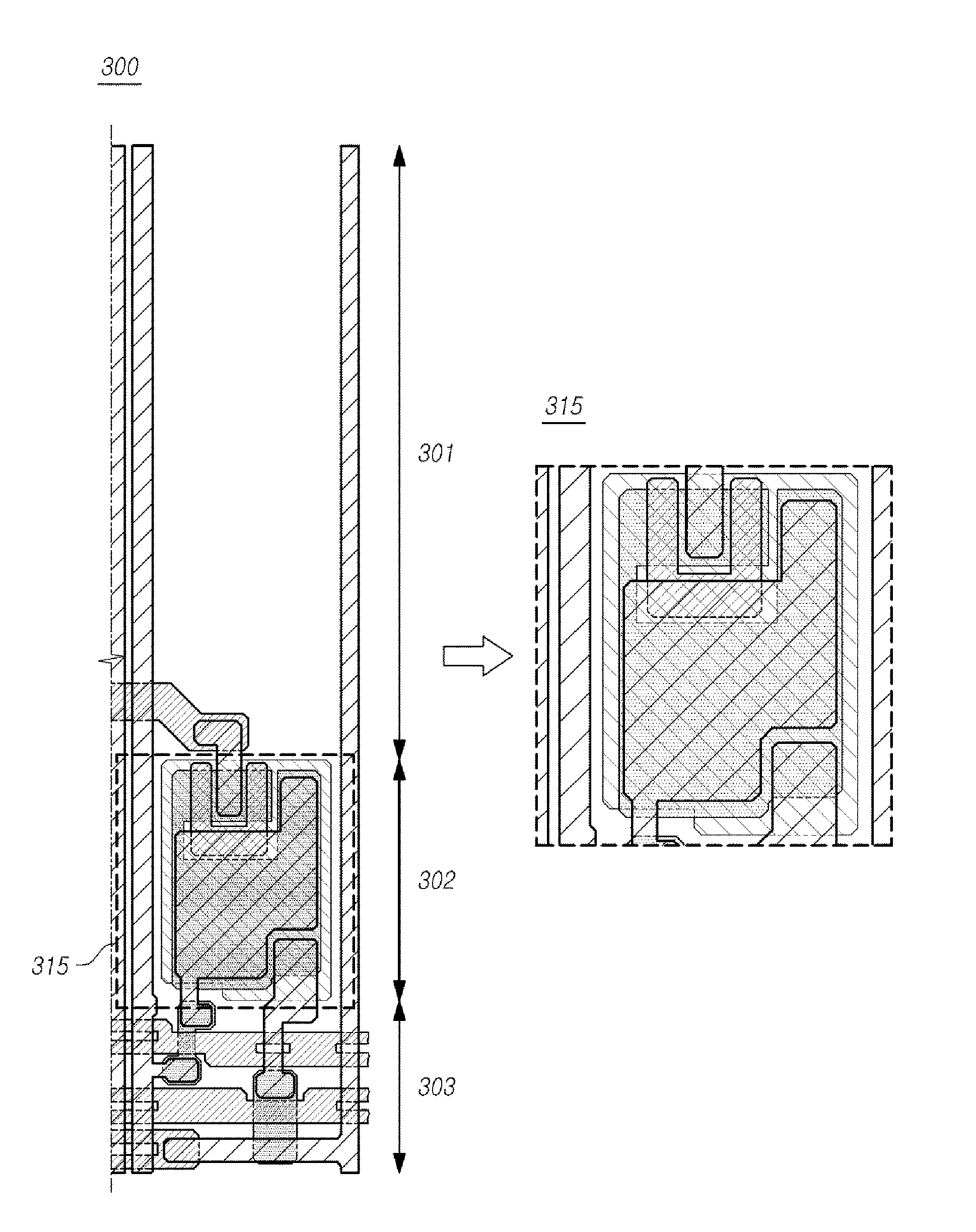
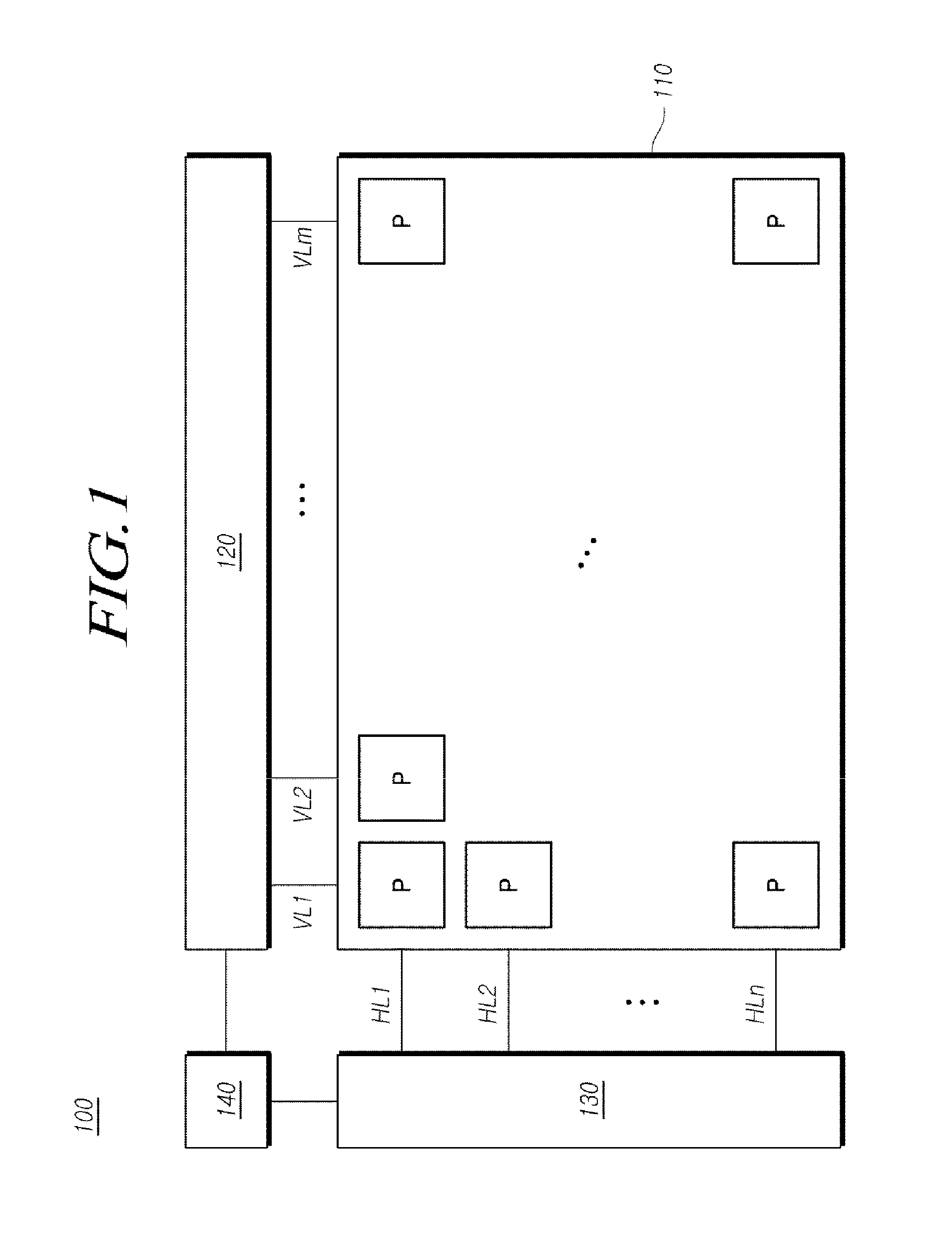
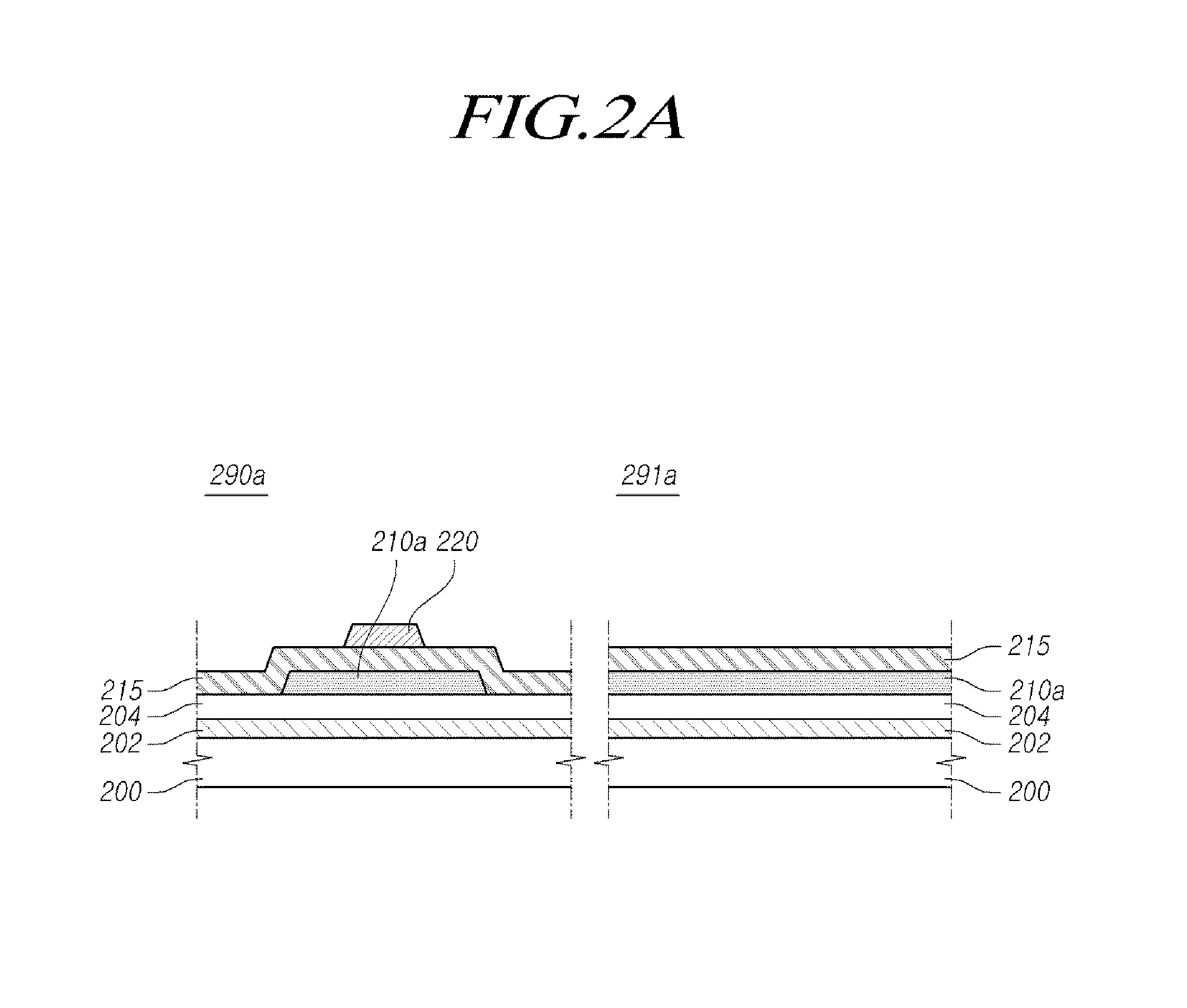
[0024]Hereinafter, exemplary embodiments of the present invention will be described with reference to the accompanying drawings. In the following description, the same elements will be designated by the same reference numerals although they are shown in different drawings. Further, in the following description of the present invention, a detailed description of known functions and configurations incorporated herein will be omitted when it may make the subject matter of the present invention rather unclear.

[0025]In addition, terms, such as first, second, A, B, (a), (b) or the like may be used herein when describing components of the present invention. Each of these terminologies is not used to define an essence, order or sequence of a corresponding component but used merely to distinguish the corresponding component from other component(s). In the case that it is described that a certain structural element “is connected to”, “is coupled to”, or “is in contact with” another structural...


PUM


Abstract

The present invention relates to an organic light emitting display panel and a method of manufacturing the same. In accordance with an aspect of the present invention, there is provided a display panel. The display panel in one example includes a light shielding layer electrically connected to a driving power line on a substrate, and storage capacitors formed on an oxide semiconductor in parallel, insulated from the oxide semiconductor, and overlapped a gate.

Description

CROSS-REFERENCE TO RELATED APPLICATION[0001]This application claims priority from and the benefit under 35 U.S.C. §119(a) of Korean Patent Application No. 10-2014-0117415, filed on Sep. 4, 2014, which is hereby incorporated by reference for all purposes as if fully set forth herein.BACKGROUND OF THE INVENTION[0002]1. Field of the Invention[0003]The present invention relates to an organic light emitting display panel and a method of manufacturing the same.[0004]2. Description of the Background Art[0005]As the information society develops, display devices for displaying an image are being increasingly required in various forms, and in recent years, various display devices such as Liquid Crystal Displays (LCDs), Plasma Display Panels (PDPs), and Organic Light Emitting Display Devices (OLEDs) have been utilized. Such a display device includes a display panel corresponding to the display device.[0006]A display panel includes thin film transistors in each pixel area, and a specific pixel ...

Claims


Application Information

Patent Timeline
Patent Type & Authority Applications(United States)
IPC IPC(8): H01L27/32H01L27/12
CPCH01L27/1225H01L27/1255H01L27/127H01L27/1262H01L27/3272H01L29/78633H10K59/1216H10K59/126H10K59/131H10K59/1213H10K59/1201
Inventor PARK, JOONGKEUNLEE, YOUNGHAK
Owner LG DISPLAY CO LTD
Why Eureka
Try Eureka