Active Matrix Organic Light-Emitting Diode Display Substrate and Display Device

Active Publication Date: 2016-03-10
BOE TECH GRP CO LTD +1
View PDF1 Cites 11 Cited by
  • Summary
  • Abstract
  • Description
  • Claims
  • Application Information

AI Technical Summary

Benefits of technology

[0017]According to the active matrix organic light-emitting diode display substrate and the display device comprising the active matrix organic light-emitting diode display substrate of the present invention, since the power signal structure comprises a power signal electrode having

Problems solved by technology

However, with an increase in resolution, every pixel 17 becomes smaller, and as a result, a relative large voltage drop may occur when the VDD wires 16 become very thin and long, which leads to different VDD vo

Method used


Image

  • Active Matrix Organic Light-Emitting Diode Display Substrate and Display Device
  • Active Matrix Organic Light-Emitting Diode Display Substrate and Display Device
  • Active Matrix Organic Light-Emitting Diode Display Substrate and Display Device

Examples


embodiment 1

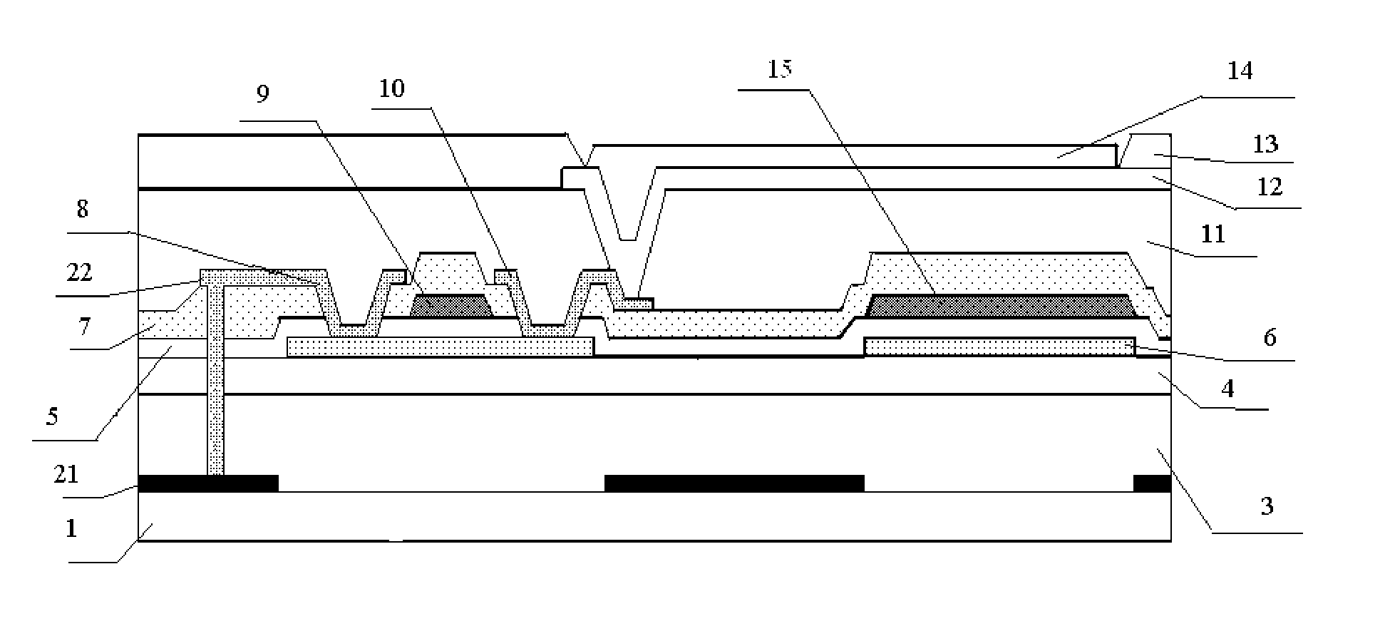
[0025]As shown in FIGS. 4 and 5, the present embodiment provides an active matrix organic light-emitting diode display substrate, which comprises a substrate 1 and a plurality of pixel structures arranged in a matrix on the substrate 1, and further comprises a power signal structure for providing a power signal for each pixel structure, wherein the power signal structure comprises one layer of power signal electrode 21 having a planar structure. Here, the “planar structure” means that the power signal electrode 21 is a separate layer in each pixel structure. It should be understood that when a thin film transistor into which a power signal is required to be input and the planar power signal electrode 21 are provided in different layers, a via hole may be provided above the power signal electrode 21 according to specific situations and the thin film transistor into which power signal is required to be input and the power signal electrode 21 are connected through the via hole.

[0026]Si...

embodiment 2

[0041]The present embodiment provides a display device, which comprises any one of the active matrix organic light-emitting diode display substrates described above.


PUM


Abstract

The present invention provides an active matrix organic light-emitting diode display substrate and a display device. The active matrix organic light-emitting diode display substrate comprises a substrate and a plurality of pixel structures arranged in a matrix on the substrate, and further comprises a power signal structure for providing a power signal to each pixel structure, wherein the power signal structure comprises one layer of power signal electrode having a planar structure. By designing the power signal structure to include a power signal electrode having a planar structure, resistance of the power signal structure is reduced, and accordingly voltage drop of VDD decreases, thus the difference in driving voltage among organic light-emitting diodes is relatively small, and uniformity of display brightness of a display panel is ensured.

Description

FIELD OF THE INVENTION[0001]The present invention relates to the field of display technology, and particularly to an active matrix organic light-emitting diode display substrate and a display device comprising the active matrix organic light-emitting diode display substrate.BACKGROUND OF THE INVENTION[0002]Driving methods for organic light-emitting displays (OLEDs) may be categorized into two types, i.e., Passive Matrix (PM) and Active Matrix (AM). Compared with PM driving methods, AM driving methods have advantages of a large amount of display information, low power consumption, long lifespan, high image contrast ratio and the like. As shown in FIG. 1, an equivalent circuit of a pixel unit of an active matrix organic light-emitting display (AMOLED) in the prior art comprises: a switching tube M1, a driving tube M2, a storage capacitor C1 and an organic light-emitting diode D1. The switching tube M1 is turned on when its gate is enabled by a scanning signal Vscan(n), and a data sign...

Claims


Application Information

Patent Timeline
IPC IPC(8): H01L27/32
CPCH01L27/3279G09G3/3225G09G2300/0426G09G2320/0233H10K59/1315
Inventor CHEN, JUNSHENG
Owner BOE TECH GRP CO LTD
Why Eureka
Try Eureka