EL Display Device

a display device and electroluminescent technology, applied in semiconductor devices, instruments, electrical apparatus, etc., can solve the problems of display screen voltage drop, etc., to suppress display screen brightness unevenness, the aperture ratio is not reduced, and the resistance of the power source line can be decreased

Active Publication Date: 2009-07-02
SHARP KK
View PDF8 Cites 22 Cited by
  • Summary
  • Abstract
  • Description
  • Claims
  • Application Information

AI Technical Summary

Benefits of technology

[0026]According to the first aspect of the present invention, the bypass line electrically connected to the power source line is arranged at the planar position of the power source line in the wiring layer, on which the signal line is also arranged, so as not to intersect the signal line. By providing such a bypass line, a resistance of the power source line can be decreased. Thus, power source voltages to be supplied to the pixel circuits become equal to one another, leading to suppression of unevenness in brightness at a display screen. Moreover, the bypass line is arranged at the planar position of the power source line in the wiring layer on which the signal line is also arranged; therefore, an additional manufacturing step for providing the bypass line is unnecessary. Further, an aperture ratio is not reduced even when the bypass line is provided. Accordingly, it is possible to decrease the resistance of the power source line without incurring increase in cost and reduction in aperture ratio and to suppress the unevenness in brightness at the display screen.
[0027]According to the second aspect of the present invention, in the EL display device in which the power source line and the scanning line are arranged so as to be orthogonal to each other, it is possible to decrease the resistance of the power source line without incurring increase in cost and reduction in aperture ratio and to suppress the unevenness in brightness at the display screen.
[0028]According to the third aspect of the present invention, the two contacts are provided at the two ends of the bypass line; therefore, the power source line and the bypass line can be electrically connected to each other with ease.
[0029]According to the fourth aspect of the present invention, by providing the single contact which is almost equal in length to the bypass line, a contact resistance can be decreased and the resistance at the portion where the power source line and the bypass line are connected in parallel can be further decreased.
[0030]According to the fifth aspect of the present invention, by providing the plurality of contacts on the almost entire part of the bypass line, the contact resistance can be decreased and the resistance at the portion where the power source line and the bypass line are connected in parallel can be further decreased. In addition, by providing the plurality of contacts each having a small size, surface roughness on the contact can be made small as compared with a case where only one contact having a large size is provided.
[0031]According to the sixth aspect of the present invention, the width of the bypass line is set to be almost equal to that of the power source line, so that the pixel circuit can be designed with ease.

Problems solved by technology

In general, however, when an electric current flows through a line having a resistive component, a voltage drop occurs.
In the active matrix-type EL display device, consequently, there is a difference in power source voltage to be supplied between a pixel circuit arranged at an end portion and a pixel circuit arranged at a center portion, so that unevenness in brightness occurs at a display screen in some instances.
Consequently, the unevenness in brightness occurs at the display screen.

Method used


Image

  • EL Display Device
  • EL Display Device
  • EL Display Device

Examples


first embodiment

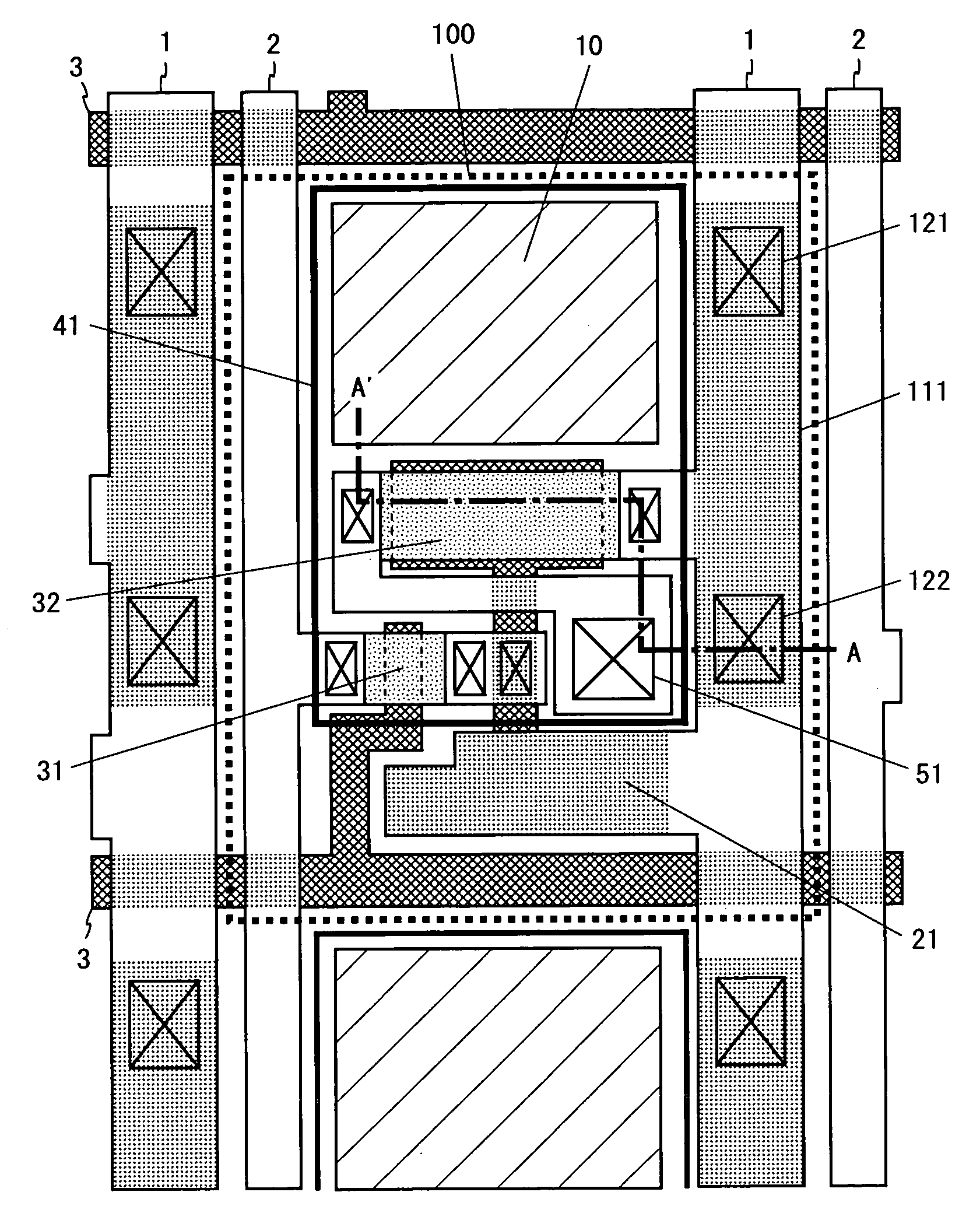
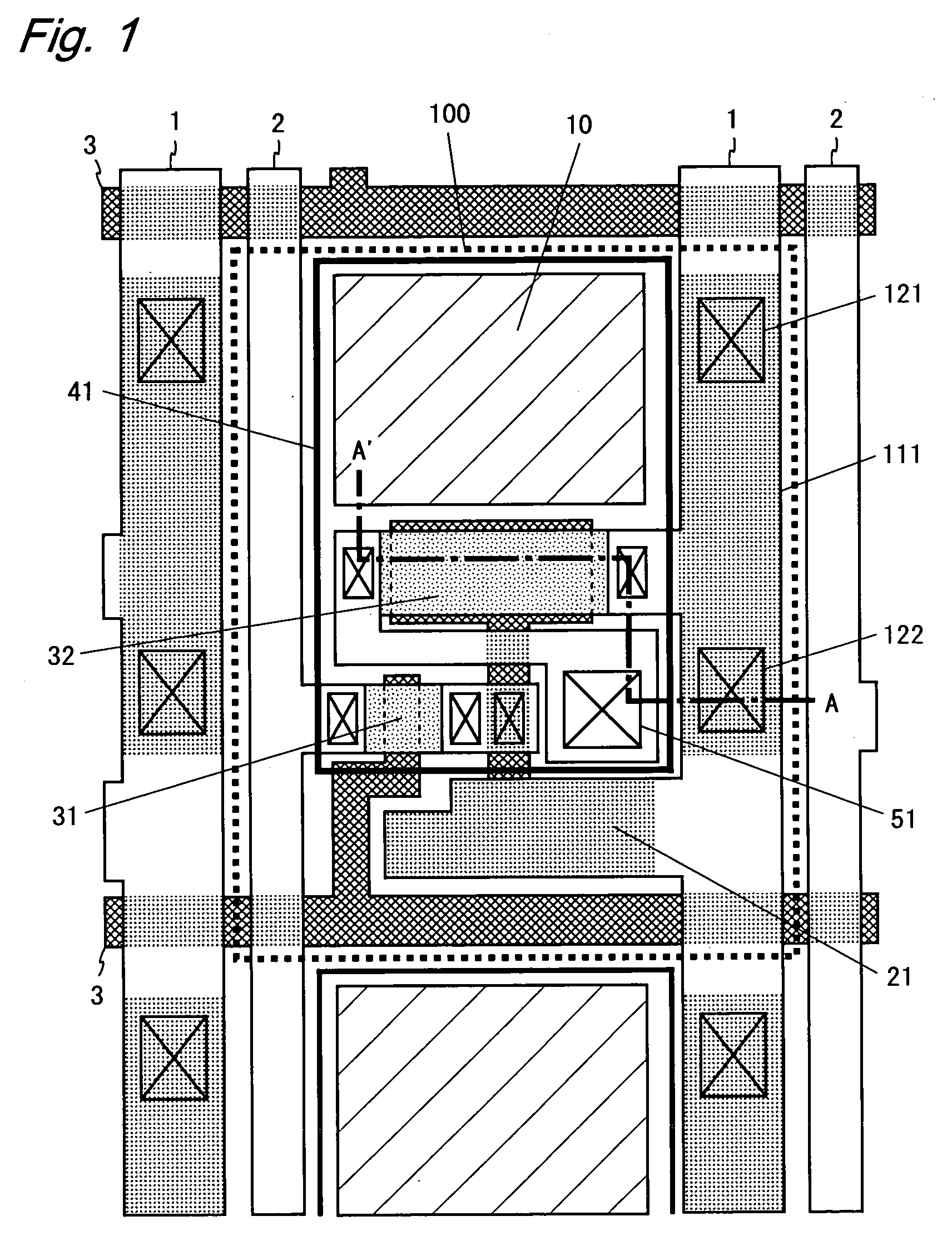
[0059]FIG. 1 is a plan view of a pixel in an EL display device according to a first embodiment of the present invention. A layout of pixels included in the EL display device according to this embodiment is shown in FIG. 1. A pixel 100 (a portion surrounded by a bold broken line) shown in FIG. 1 functions as one pixel in an EL display device that performs monochromatic display, and functions as a sub pixel corresponding to one color in an EL display device that performs color display. The EL display device according to this embodiment is an active matrix-type EL display device having a plurality of pixels 100 arranged two-dimensionally.

[0060]As shown in FIG. 1, the EL display device according to this embodiment includes a plurality of power source lines 1, a plurality of data lines 2 and a plurality of scanning lines 3. These lines are arranged on one of two wiring layers: upper and lower wiring layers. Of the upper and lower wiring layers, hereinafter, the lower wiring layer (a wiri...

sixth embodiments

Second to Sixth Embodiments

[0081]EL display devices according to second to sixth embodiments are almost equal in configuration to the EL display device according to the first embodiment. In the following, therefore, constituent elements identical with those in the first embodiment are denoted by the identical reference symbols and description thereof will not be given, and description will be given of differences between the second to sixth embodiments and the first embodiment.

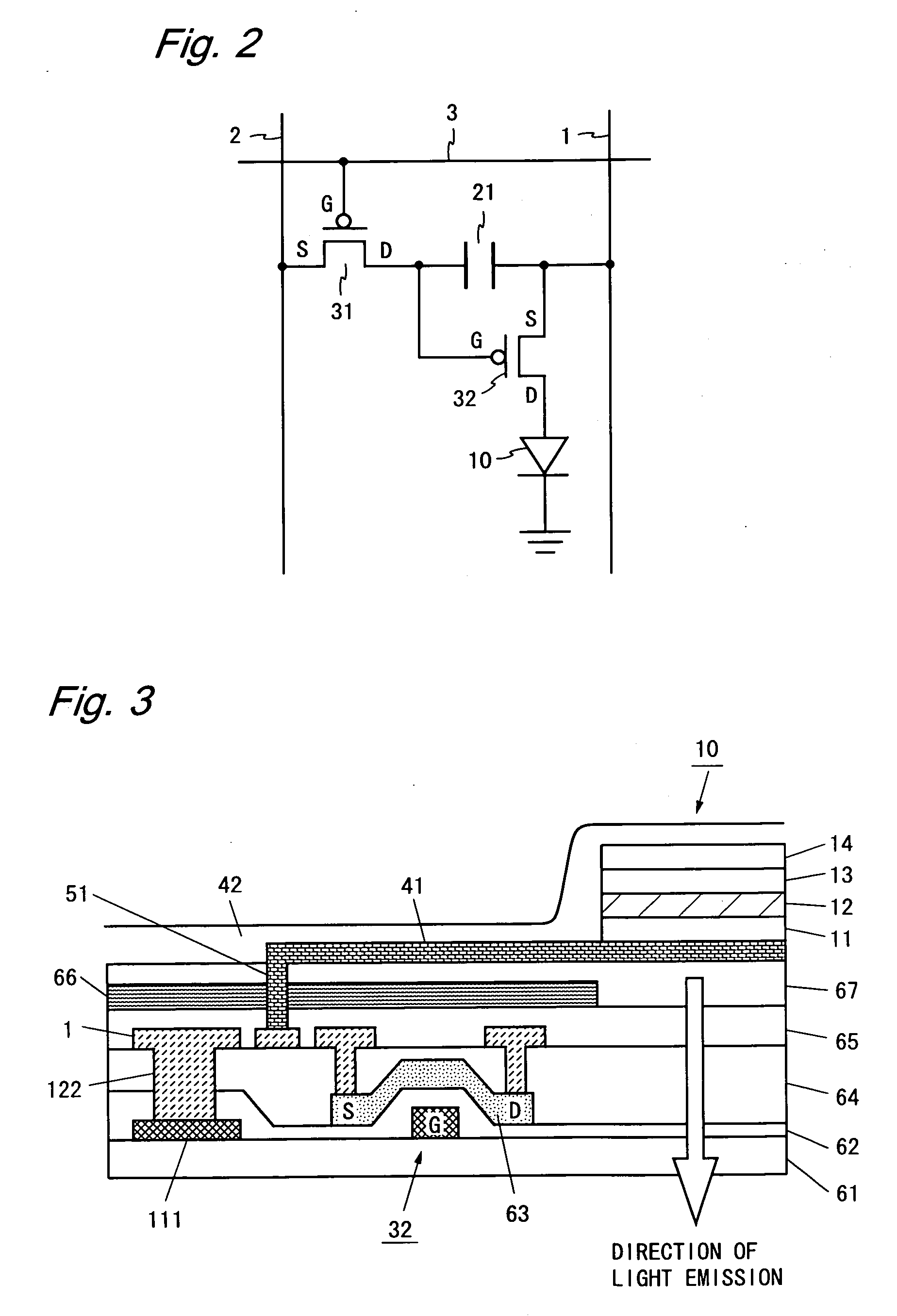
[0082]FIG. 4 is a plan view of a pixel in the EL display device according to the second embodiment of the present invention. A pixel 200 shown in FIG. 4 includes one contact 221 which is almost equal in length to the bypass line 111, in place of the two contacts 121 and 122. The contact 221 can be formed by a method which is equal to that for the contacts 121 and 122.

[0083]In the EL display device according to the second embodiment, as described above, by providing the single contact 221 which is almost equal ...


PUM


Abstract

A power source line 1 and a scanning line 3 are arranged on different wiring layers so as to be orthogonal to each other. In the wiring layer on which the scanning line 3 is arranged, a bypass line 111 is arranged on at least a part of a portion obtained by removing a planar position of the scanning line 3 from a planar position of the power source line 1. Contacts 121 and 122 establish electric connection between the power source line 1 and the bypass line 111. As described above, the bypass line 111 is connected to the power source line 1 in parallel, leading to decrease in resistance of the power source line 1 and suppression of unevenness in brightness at a display screen. Moreover, an additional manufacturing step for providing the bypass line 111 is unnecessary. Further, an aperture ratio is not reduced even when the bypass line 111 is provided. When the bypass line 111 is made wider than the power source line 1, a pixel circuit can be prevented from operating erroneously due to external light.

Description

TECHNICAL FIELD[0001]The present invention relates to an electroluminescence display device. In particular, the present invention relates to an active matrix-type electroluminescence display device in which pixel circuits each including an electroluminescence element and a thin-film transistor(s) are arranged two-dimensionally.BACKGROUND ART[0002]As a self-luminous display device, recently, attention has been given to an electroluminescence (EL) display device using an EL element. In addition, there has also been developed an active matrix-type EL display device in which pixel circuits each including an EL element and a thin-film transistor (TFT) are arranged two-dimensionally.[0003]An organic EL element, which is one example of EL elements, has a sandwich structure in which a light emitting layer made of an organic substance is interposed between an anode and a cathode. In the organic EL element, when a voltage is applied between the anode and the cathode, holes are injected from t...

Claims


Application Information

Patent Timeline
Patent Type & Authority Applications(United States)
IPC IPC(8): G09G3/30
CPCH01L27/3248H01L27/124H01L29/78633H01L27/3276H10K59/123H10K59/131
Inventor KISHI, NORITAKA
Owner SHARP KK
Why Eureka
Try Eureka