
Electro-optical device and electronic apparatus

a technology applied in the field of optical devices and electronic devices, can solve the problems of difficulty in simultaneously and achieve the effects of increasing the capacitance value of storage capacitors, enhancing display performance, and reducing the size of opening regions

Active Publication Date: 2016-03-17
138 EAST LCD ADVANCEMENTS LTD
View PDF0 Cites 7 Cited by
  • Summary
  • Abstract
  • Description
  • Claims
  • Application Information

AI Technical Summary

Benefits of technology

This approach enhances the display performance by increasing the capacitance value of the storage capacitor while maintaining or enlarging the opening region, thereby improving image quality and contrast.

Problems solved by technology

Accordingly, it is technically difficult to simultaneously increase the capacitance value of the storage capacitor and size of the opening region, and thus there is a technical problem in enhancing the display performance of an electro-optical device such as a liquid crystal device.

Method used


Image

  • Electro-optical device and electronic apparatus
  • Electro-optical device and electronic apparatus
  • Electro-optical device and electronic apparatus

Examples


first embodiment

1-1: Overall Configuration of Liquid Crystal Device

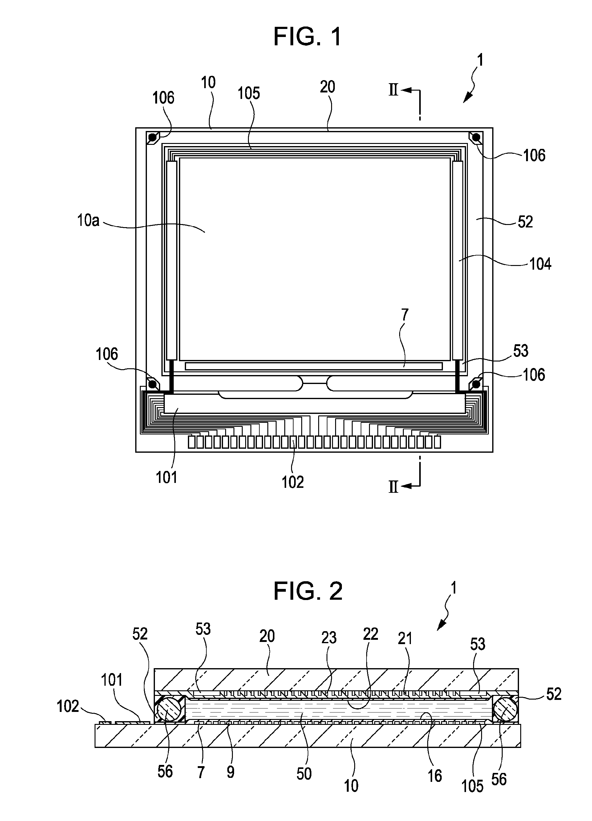
[0062]First, the overall configuration of a liquid crystal device 1 according to this embodiment will be described with reference to FIGS. 1 and 2.

[0063]FIG. 1 is a plan view showing the overall configuration of the liquid crystal device 1 according to this embodiment. FIG. 2 is a cross-sectional view taken along a line II-II in FIG. 1.

[0064]Referring to FIGS. 1 and 2, the liquid crystal device 1 includes a TFT-array substrate 10 and an opposing substrate 20 which are disposed opposite to each other. The TFT-array substrate 10 is an example of a substrate according to the invention. The TFT-array substrate 10 is, for example, a transparent substrate such as a quartz substrate or a glass substrate, or a silicon substrate. The opposing substrate 20 is a substrate made of, for example, the same material as the TFT-array substrate 10. Between the TFT-array substrate 10 and the opposing substrate 20, liquid crystal is encapsulated to for...

modified example

[0095]Next, a modified example of the liquid crystal device 1 according to this embodiment will be described with reference to FIG. 8. FIG. 8 is a cross-sectional view showing the configuration of the modified example of the liquid crystal device according to this embodiment, and is a partial cross-sectional view taken by cutting the liquid crystal device according to the modified example in the cross section corresponding to FIG. 7. In this instance, common parts to the liquid crystal device 1 are designated by same reference numerals, and the detailed description thereof will be omitted.

[0096]In FIG. 8, the liquid crystal device according to this embodiment is different from the above-described liquid crystal device 1, except for a relay layer 7a, data lines 6a, contact holes 33a, 34, 35 and 36, insulation films 17 and 18 and a dielectric film 72a.

[0097]The dielectric film 72a is made of alumina, similar to the dielectric film 72, and constitutes the storage capacitor 70 together...

second embodiment

[0101]Next, a liquid crystal device according to the second embodiment will be described with reference to FIGS. 9 to 11. In this instance, the second embodiment is substantially identical to the first embodiment, except for some configurations. For this reason, in the second embodiment, the portions different from those of the first embodiment will be described in detail, and the same portions will be not described herein.

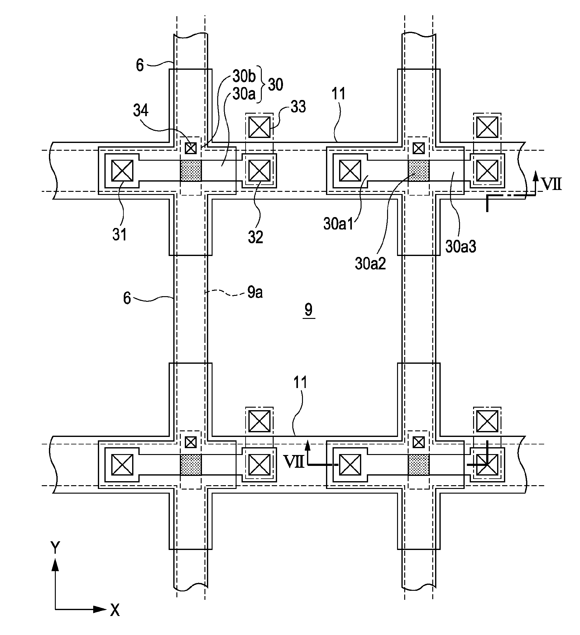
[0102]FIGS. 9 and 10 are plan views transparently showing a positional relationship of the respective layers constituting the liquid crystal device according to the second embodiment. FIG. 11 is a cross-sectional view showing a laminate structure of the liquid crystal device according to the second embodiment. In this instance, in FIG. 9, each layer lower than the relay layer 91 and 92 is shown, and in FIG. 10, each layer higher than the relay layer 91 and 92 is shown. Further, in FIGS. 9 to 11, each of the layers and each of the members are shown in different sca...


PUM

PropertyMeasurementUnit
contrast ratioaaaaaaaaaa
angleaaaaaaaaaa
contrastaaaaaaaaaa

Abstract

An electro-optical device includes a first light shielding film; a transistor element formed on the first light shielding film to overlap the first light shielding film; a second light shielding film formed on the transistor element to overlap the transistor element and electrically connected to an input terminal of the transistor element; a transparent conductive film extended toward an upper layer side of the second light shielding film in an opening region, through which light penetrates, of the display region; a dielectric film formed on the transparent conductive film in the opening region; and a transparent pixel electrode formed on the dielectric film in the opening region, constituting a storage capacitor together with the transparent conductive film and the dielectric film, and having a transparent pixel electrode which is electrically connected to the transistor element.

Description

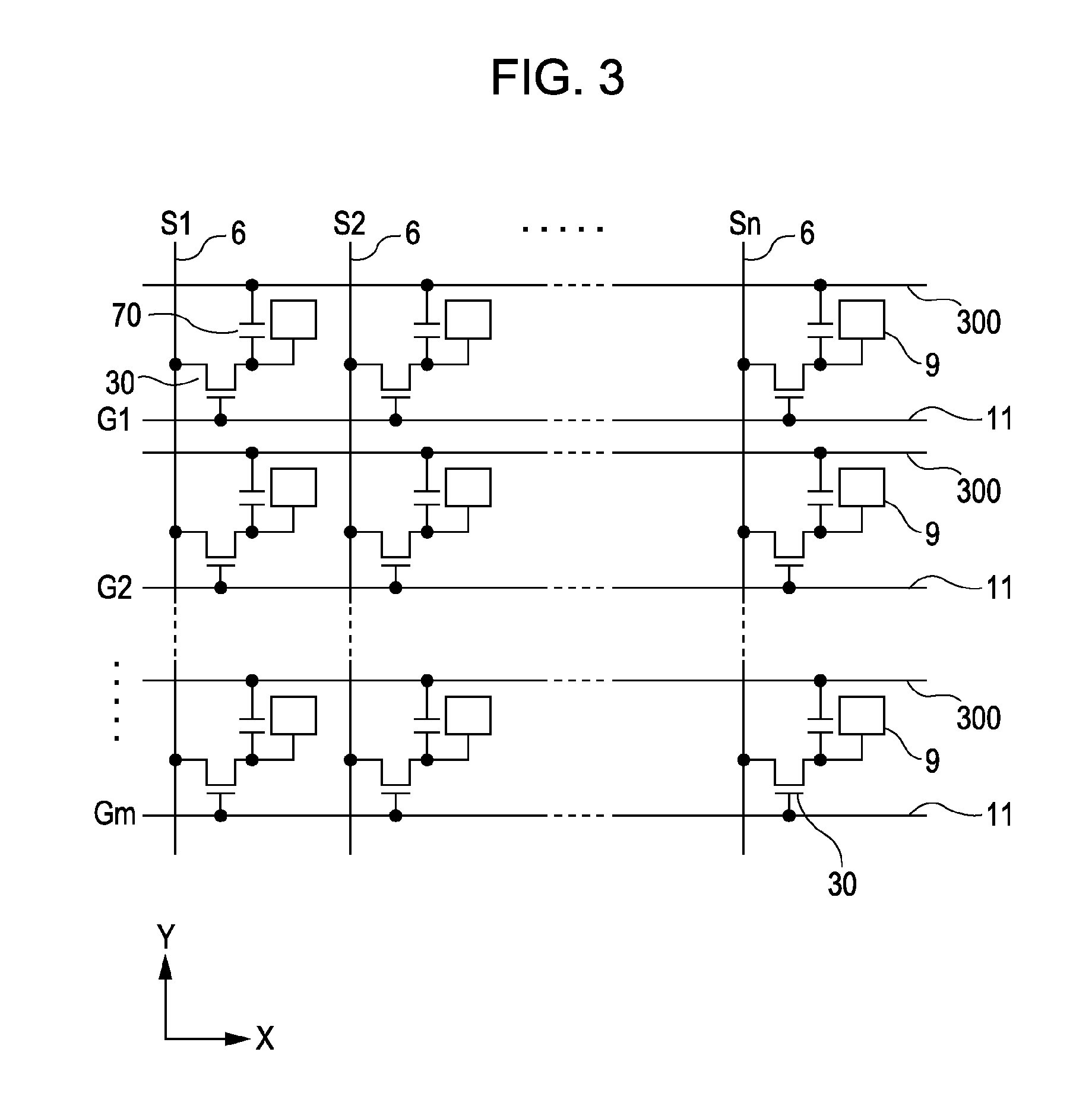
CROSS-REFERENCE TO RELATED APPLICATIONS[0001]This application is a divisional of U.S. patent application Ser. No. 12 / 652,277, filed Jan. 5, 2010, which claims priority to Japanese Patent Application No. 2009-000277, filed Jan. 5, 2009 and Japanese Patent Application No. 2009-259898, filed Nov. 13, 2009. The foregoing applications are incorporated herein.BACKGROUND[0002]1. Technical Field[0003]The present invention relates to an electro-optical device including thin film transistors which are disposed for every pixel on an element substrate as a switching element, such as a liquid crystal device, and an electronic apparatus including the electro-optical device, such as a liquid crystal projector.[0004]2. Related Art[0005]Such an electro-optical device includes pixel electrodes, scanning lines for selectively driving the pixel electrodes, data lines and a TFT (Thin Film Transistor) as a pixel switching element, which are provided on a substrate, to deliver the active matrix drive. In ...

Claims


Application Information

Patent Timeline
Patent Type & Authority Applications(United States)
IPC IPC(8): G02F1/1362G02F1/1333G02F1/1368
CPCG02F1/136213G02F1/136286G02F1/136227G02F1/133345G02F1/1368H01L27/1255H01L29/78633H01L27/124G02F2201/123
Inventor IKI, TAKUNORI
Owner 138 EAST LCD ADVANCEMENTS LTD
Learn More