Wafer processing method

Active Publication Date: 2016-03-24
DISCO CORP
View PDF1 Cites 0 Cited by
  • Summary
  • Abstract
  • Description
  • Claims
  • Application Information

AI Technical Summary

Benefits of technology

The present invention is a wafer processing method that reduces vibrations and prevents burrs during cutting. The method involves using a cutting blade and a dicing tape with adhesive film to cut the wafer along division lines. The cutting blade has its cutting edge positioned to cut into the cured adhesive layer, which supports the cutting edge and reduces vibrations that could lead to damage. The cutting blade is positioned in a way that prevents the base sheet of the dicing tape from being cut, reducing the likelihood of wire breaking.

Problems solved by technology

Accordingly, burrs are generated from the base sheet and stick to the adhesive film, causing breaking of wire in bonding each device to a wiring board.

Method used


Image

  • Wafer processing method
  • Wafer processing method
  • Wafer processing method

Examples


Embodiment Construction

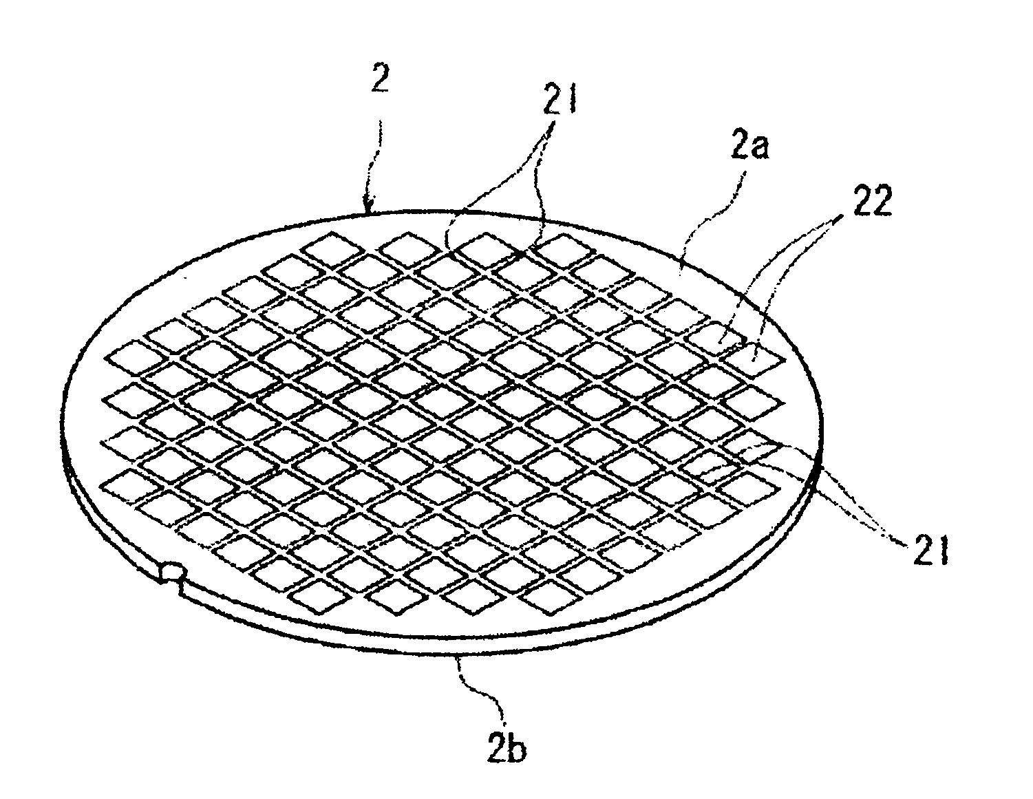
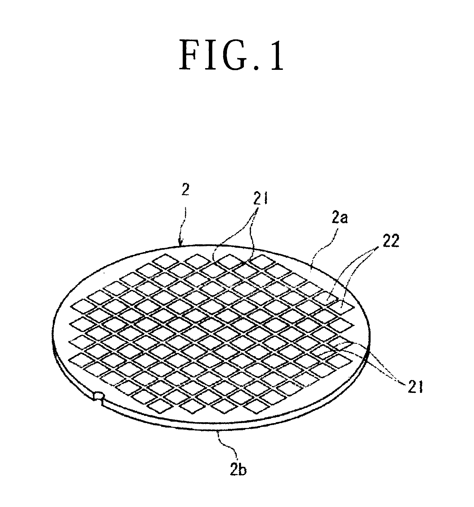
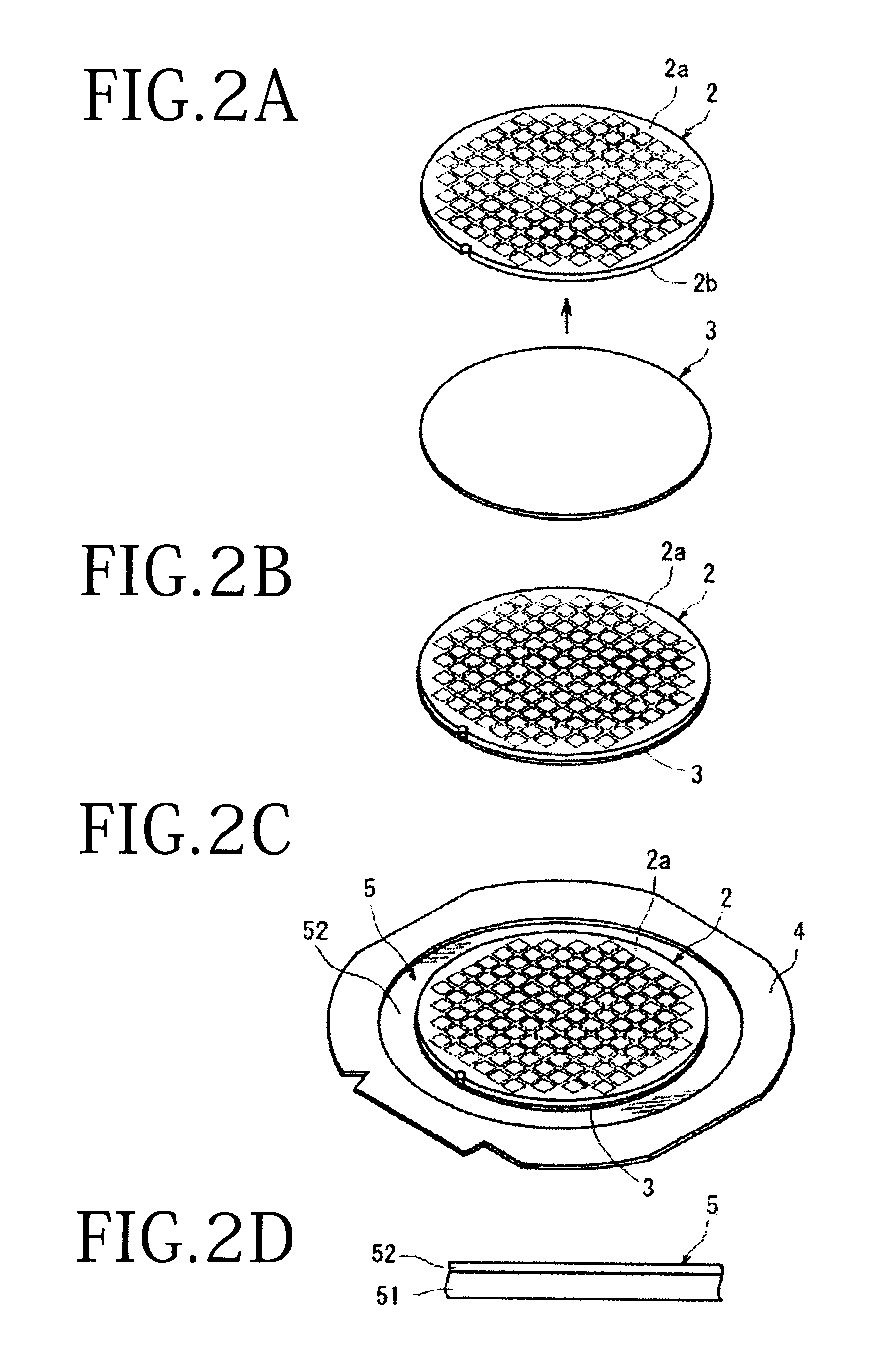
[0020]A preferred embodiment of the wafer processing method according to the present invention will now be described in detail with reference to the attached drawings. FIG. 1 is a perspective view of a semiconductor wafer 2. The semiconductor wafer 2 shown in FIG. 1 is a silicon wafer having a thickness of 200 μm, for example. The semiconductor wafer 2 has a front side 2a and a back side 2b. A plurality of division lines 21 are formed on the front side 2a of the semiconductor wafer 2 to thereby define a plurality of separate regions where a plurality of devices 22 such as ICs and LSIs are formed. There will now be described a wafer processing method of dividing the semiconductor wafer 2 along the division lines 21 to obtain the individual devices 22 as chips and mounting an adhesive film for die bonding on the back side of each device 22.

[0021]First, a wafer supporting step is performed in such a manner that one side of the adhesive film is mounted on the back side of the wafer and ...


PUM


Abstract

A wafer is divided along a plurality of crossing division lines to obtain a plurality of individual devices. The division lines are formed on the front side of the wafer to define a plurality of separate device regions. An adhesive film is applied to the back side of the wafer and the other side of the adhesive film is attached to a dicing tape composed of a base sheet and an ultraviolet curable adhesive layer formed on the base sheet. The adhesive film is attached to the ultraviolet curable adhesive layer of the dicing tape. Ultraviolet light is applied to the dicing tape to thereby cure the adhesive layer. A rotating cutting blade cuts the wafer together with the adhesive film along the division lines, dividing the wafer into the individual devices. The cutting blade is positioned so that its cutting edge cuts into the cured adhesive layer.

Description

BACKGROUND OF THE INVENTION[0001]1. Field of the Invention[0002]The present invention relates to a wafer processing method of dividing a wafer along a plurality of division lines to obtain a plurality of individual devices and mounting an adhesive film for die bonding on the back side of each device, the division lines being formed on the front side of the wafer to thereby define a plurality of separate regions where the respective devices are formed.[0003]2. Description of the Related Art[0004]In a semiconductor device fabrication process, a plurality of crossing division lines are formed on the front side of a substantially disk-shaped semiconductor wafer to thereby define a plurality of separate regions where a plurality of devices such as ICs and LSIs are formed. An adhesive film for die bonding called die attach film (DAF) is mounted on the back side of the semiconductor wafer having the devices on the front side. The adhesive film is formed of polyimide resin, epoxy resin, or ...

Claims


Application Information

Patent Timeline
IPC IPC(8): H01L21/78
CPCH01L21/78H01L21/6836H01L2221/68354H01L2221/68327H01L2221/68377
Inventor NAKAMURA, MASARU
Owner DISCO CORP
Why Eureka
Try Eureka