Electro-optical device and electronic instrument

a technology of electro-optical devices and electronic instruments, applied in the direction of non-linear optics, identification means, instruments, etc., can solve the problems of inability to obtain desired optical characteristics, relatively easy to occur display unevenness, and formation of electro-optical devices in which display unevenness occurs easily with respect to simple shifts in assembly, etc., to achieve the effect of suppressing image luminance unevenness

Active Publication Date: 2016-04-21
SEIKO EPSON CORP
View PDF0 Cites 19 Cited by
  • Summary
  • Abstract
  • Description
  • Claims
  • Application Information

AI Technical Summary

Benefits of technology

[0014]An advantage of some aspects of the invention is to provide an electro-optical device that can suppress luminance unevenness of images even if positional shifts occur when pasting a lens array substrate and an element substrate together, and an electronic instrument that is provided with the electro-optical device.
[0017]An advantage of some aspects of the invention is to provide an electro-optical device that can suppress luminance unevenness of images even if positional shifts occur when pasting a first substrate, on which pixel electrodes are formed, and a second substrate, on which optical elements such as a lens are formed, together, and an electronic instrument that is provided with the electro-optical device.
[0020]In this case, since the positions of the second opening components of the other substrate are corrected with the positions of the first opening components of the one substrate set as references, in comparison with a case in which correction is not carried out, it is possible to set an allowable amount of relative positional shift of both substrates to be larger when configuring an electro-optical device by pasting the one substrate and the other substrate together. In addition, even if incidence light, which is incident to the pixel region, has an intensity distribution as a result of incidence angles, in a case in which an optical axis of the incidence light is set so as to pass through a core of the pixel region, it is possible to provide an electro-optical device in which it is difficult for display unevenness to occur as an effect of the intensity distribution of the incidence light.
[0022]In this case, since the correction values are set for each of the plurality of correction regions in each of the plurality of pixels, the correction of positions of the second opening components is easily performed in comparison with a case that is applied by determining correction values.
[0024]In this case, in a case in which the optical axis of incidence light is set to pass through the core of the pixel region, since it is difficult for the intensity as a result of incidence angles of incidence light that is incident to the pixel region to fluctuate about the optical axis, it is difficult for display unevenness to occur even if correction values in a correction region that includes the core of the pixel region are set to be zero. In other words, the realization of still simpler correction of the positions of the second opening components is possible.
[0028]In this case, the plurality of first lenses and the plurality of second lenses oppose the plurality of pixel electrodes with a one-to-one relationship, but the cores of the first lenses are shifted to an outer side in the first direction with respect to the cores of the pixel electrodes at end section sides in the first direction of a region in which the pixel electrodes are arranged. Therefore, when the electro-optical device is irradiated with light, even in a case in which the intensity of light that is incident to the electro-optical device in an oblique manner from an outer side is higher than that of light that is incident to the electro-optical device in an oblique manner from an inner side, the light is condensed at substantial centers of the pixel electrodes. Accordingly, when an electro-optical device is produced, it is even possible to suppress the occurrence of a circumstance in which the luminance of an image is partially reduced when the element substrate is pasted together with the lens array substrate in a state that is shifted in the first direction.

Problems solved by technology

Although the pair of substrates are pasted together at a predetermined position using a general adhesive, if the pair of substrates are bonded to the predetermined position shifted by more than is allowed, there is a problem in that it is not possible to obtain desired optical characteristics.
However, if the pitch of pixels of one substrate is corrected in consideration of amounts of shift that are caused by the thermal expansion of the pair of substrates, it is relatively easy for display unevenness to occur as a result of deteriorations in the abovementioned transmittance in a case in which there are shifts in the positioning in the pair of substrates other than deformations due to thermal expansion.
In other words, there is a concern that an electro-optical device in which display unevenness occurs easily with respect to mere shifts in assembly, will be formed.
Therefore, even if the manufacturing method of the electro-optical device of JP-A-2004-61633 is used, it is not possible to effectively improve the abovementioned deterioration in transmittance, and therefore, there is a concern that display unevenness will become significant.
The abovementioned problem is difficult to solve using the technology that is disclosed in JPA-2004-61633.
The abovementioned problem is difficult to solve using the technology that is disclosed in JP-A-2004-61633.
In this case, in a case in which the optical axis of incidence light is set to pass through the core of the pixel region, since it is difficult for the intensity as a result of incidence angles of incidence light that is incident to the pixel region to fluctuate about the optical axis, it is difficult for display unevenness to occur even if correction values in a correction region that includes the core of the pixel region are set to be zero.

Method used


Image

  • Electro-optical device and electronic instrument
  • Electro-optical device and electronic instrument
  • Electro-optical device and electronic instrument

Examples


embodiment 1

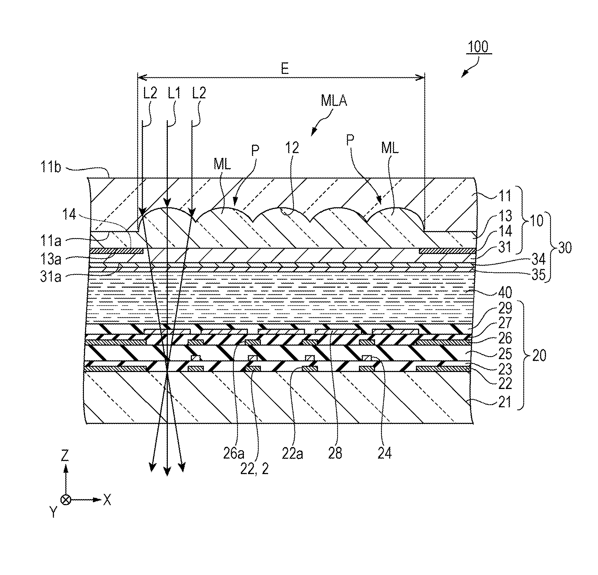
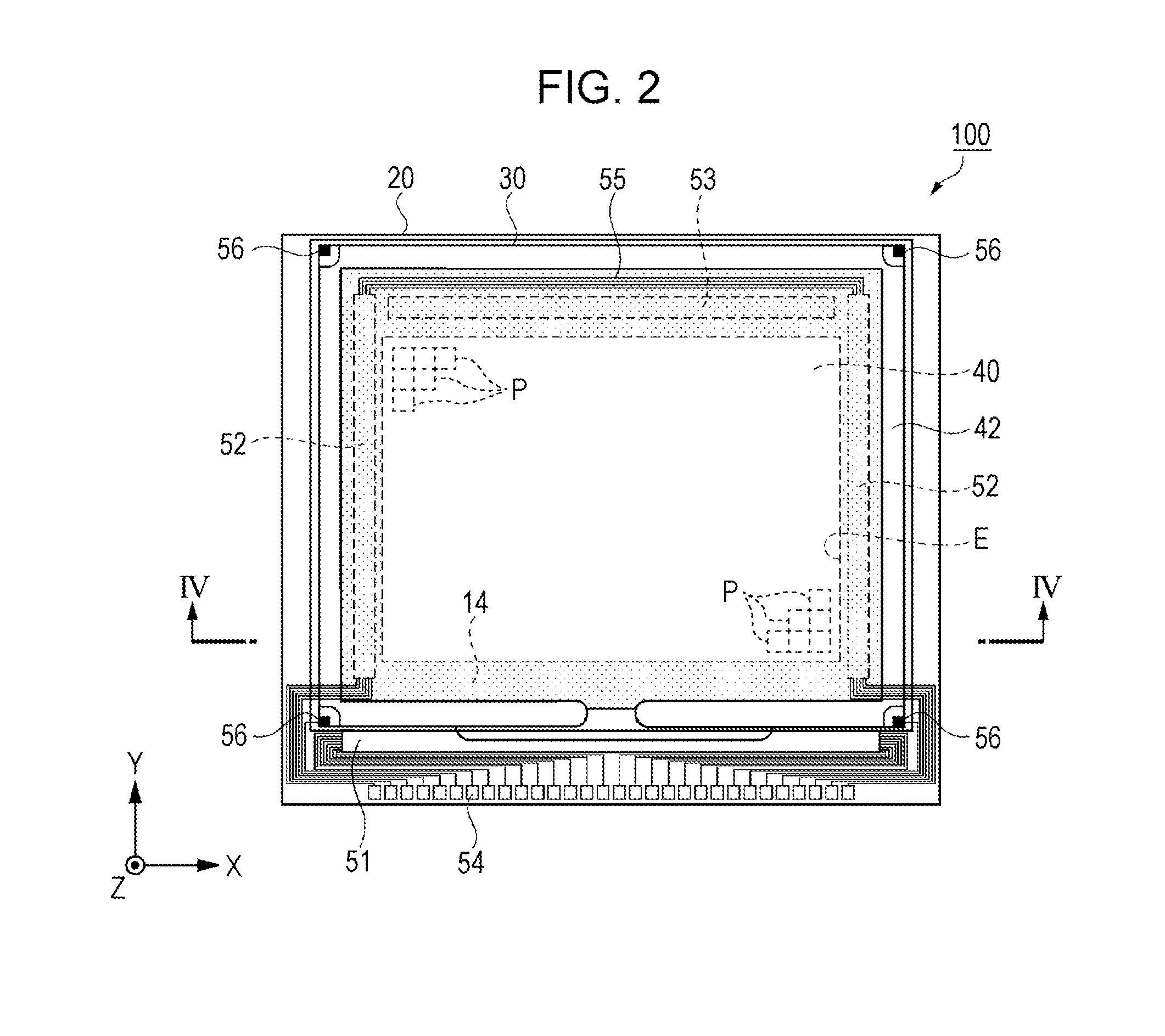
[0111]In the present embodiment, description is given using an active matrix type liquid crystal device as an example of an electro-optical device that is provided with a thin film transistor (TFT) as a switching element of a pixel. It is possible to use the liquid crystal device suitably as an optical modulation element (a liquid crystal light bulb) of a projection type display device (a liquid crystal projector) that will be described below.

Electronic Instrument

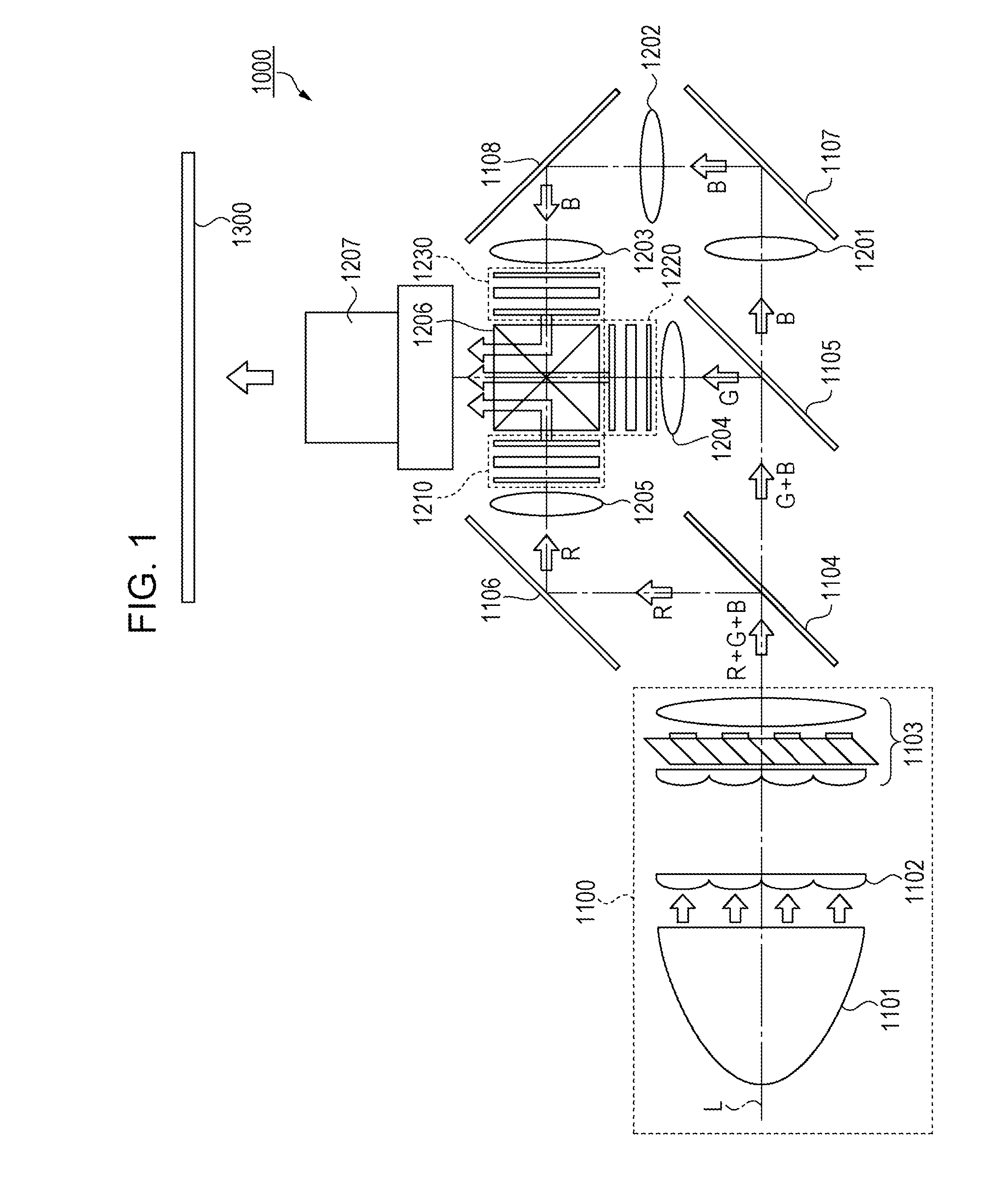
[0112]Firstly, a projection type display device will be described with reference to FIG. 1 as an electronic instrument in which a liquid crystal device is adopted as the electro-optical device of the present embodiment. FIG. 1 is a schematic diagram that shows a configuration of a projection type display device.

[0113]As shown in FIG. 1, a projection type display device 1000, as the electronic instrument of the present embodiment, is provided with a polarized light illumination device 1100 that is disposed along a system opt...

modification example 1

[0205]The second opening components in the pixels P are not limited to opening sections Pm that are stipulated by the microlenses ML and the light shielding films 14. FIG. 13 is a schematic plan view that shows second opening components (opening sections Pm) of a Modification Example. As shown in FIG. 13, the second opening components (the opening sections Pm) in the opposing substrate 30 need not have the microlenses ML, and may be black matrices (BM) that extend in a lattice from in the X direction and the Y direction. In addition, the second opening components may be prisms that condense incidence light into an opening region of the pixels P, or color filters that convert incidence light into colored light. Furthermore, the second opening components may be configured to combine the microlenses ML, prisms, or color filters with the abovementioned black matrices (BM).

modification example 2

[0206]In the abovementioned embodiment, an example in which the microlenses ML that configure the opening components were provided on the opposing substrate 30 side was shown, but it is also possible to apply the correction method of the positions of opening components of the present application in a case in which the microlenses ML or prisms that configure the opening components are provided on the element substrate 20 side, and light is incident from the element substrate 20 side. In addition, a configuration in which the microlenses ML and prisms are respectively provided on the element substrate 20 and the opposing substrate 30 is also possible. In either case, the opening components that are positioned on an incidence side of light are set as the second opening components.


PUM

PropertyMeasurementUnit
frequencyaaaaaaaaaa
transmittanceaaaaaaaaaa
refractive indexaaaaaaaaaa

Abstract

An electro-optical device of the present embodiment includes a pair of substrates, first opening components that stipulate sizes and positions of opening sections of pixels in one of the pair of substrates, and second opening components (microlenses) that stipulate sizes and positions of opening sections of the pixels in the other of the pair of substrates. Positions of the second opening components (microlenses) of the other substrate are corrected with positions of the first opening components of the one substrate set as references, so as to gradually become more shifted in a direction that runs from a core of a pixel region, in which a plurality of pixels are arranged, toward an edge section of the pixel region, in accordance with separation from a core side of the pixel region.

Description

BACKGROUND[0001]1. Technical Field[0002]The present invention relates to an electro-optical device and an electronic instrument.[0003]2. Related Art[0004]Liquid crystal display devices as electro-optical devices are capable of displaying by disposing a pair of substrates opposite to one another, interposing a liquid crystal layer in a gap therebetween, and configuring a plurality of pixels. Although the pair of substrates are pasted together at a predetermined position using a general adhesive, if the pair of substrates are bonded to the predetermined position shifted by more than is allowed, there is a problem in that it is not possible to obtain desired optical characteristics.[0005]In response to this kind of problem, for example, JP-A-2004-61633 discloses a manufacturing method of an electro-optical device that includes pasting together substrates in which the pitch of the pixels of at least one substrate, among a pair of substrates in which pixels are configured in a matrix for...

Claims


Application Information

Patent Timeline
Patent Type & Authority Applications(United States)
IPC IPC(8): G02F1/1335G03B21/00G02F1/1343G02B3/00
CPCG02F1/133526G02B3/0056G02B3/0068G02F1/134336G02F1/133512G02F1/133514G03B21/006G03B21/14G09F9/35G02F1/133567H04N9/3105
Inventor TATENO, YOSHITAKEMIYAWAKI, DAISUKETANI, TOSHIKINAKAGAWA, MASASHI
Owner SEIKO EPSON CORP
Why Eureka
Try Eureka