Mask blank substrate, mask blank, transfer mask, and method of manufacturing semiconductor device

a technology of mask blank substrate and transfer mask, which is applied in the direction of photomechanical equipment, instruments, originals for photomechanical treatment, etc., can solve the problem of reducing the allowable focus latitude, the influence of lens aberration of the projection optical system on the transfer accuracy is becoming greater, and the principal surface of the transparent substrate is limited in the increase of flatness, so as to reduce the facility cost of manufacturing devices, the effect of high substantial flatness

Active Publication Date: 2016-04-21
HOYA CORP
View PDF1 Cites 14 Cited by
  • Summary
  • Abstract
  • Description
  • Claims
  • Application Information

AI Technical Summary

Benefits of technology

[0040]According to this invention, by selecting using a reference value where the mechanical flatness is replaced by the optical flatness, a mask blank substrate can be obtained which satisfies the requirement of an extremely high substantial flatness of one-eighth of an exposure wavelength λ. This makes it possible to manufacture such an ultra-flat mask blank substrate without reducing the manufacturing throughput of the mask blank substrate, and also reducing facility cost of manufacturing devices. Effective flatness of the mask blank and the transfer mask can be made higher, similar to the mask blank substrate. When exposed using the transfer mask, focus latitude and high positional precision are assured, and extremely high transfer accuracy can be obtained. As a result, the circuit operation characteristic of the semiconductor device to be manufactured is stabilized.

Problems solved by technology

Therefore, reduction in the mask surface flatness causes a decrease in allowable focus latitude.
However, there is a limitation in increasing flatness of the principal surface of the transparent substrate in its polishing using conventional double side polishing apparatus.
Further, there is a problem that the influence of the lens aberration of the projection optical system on transfer accuracy is becoming greater due to a decrease in focus latitude in the lithography process together with an increase in NA of exposure apparatus.

Method used


Image

  • Mask blank substrate, mask blank, transfer mask, and method of manufacturing semiconductor device
  • Mask blank substrate, mask blank, transfer mask, and method of manufacturing semiconductor device
  • Mask blank substrate, mask blank, transfer mask, and method of manufacturing semiconductor device

Examples


examples

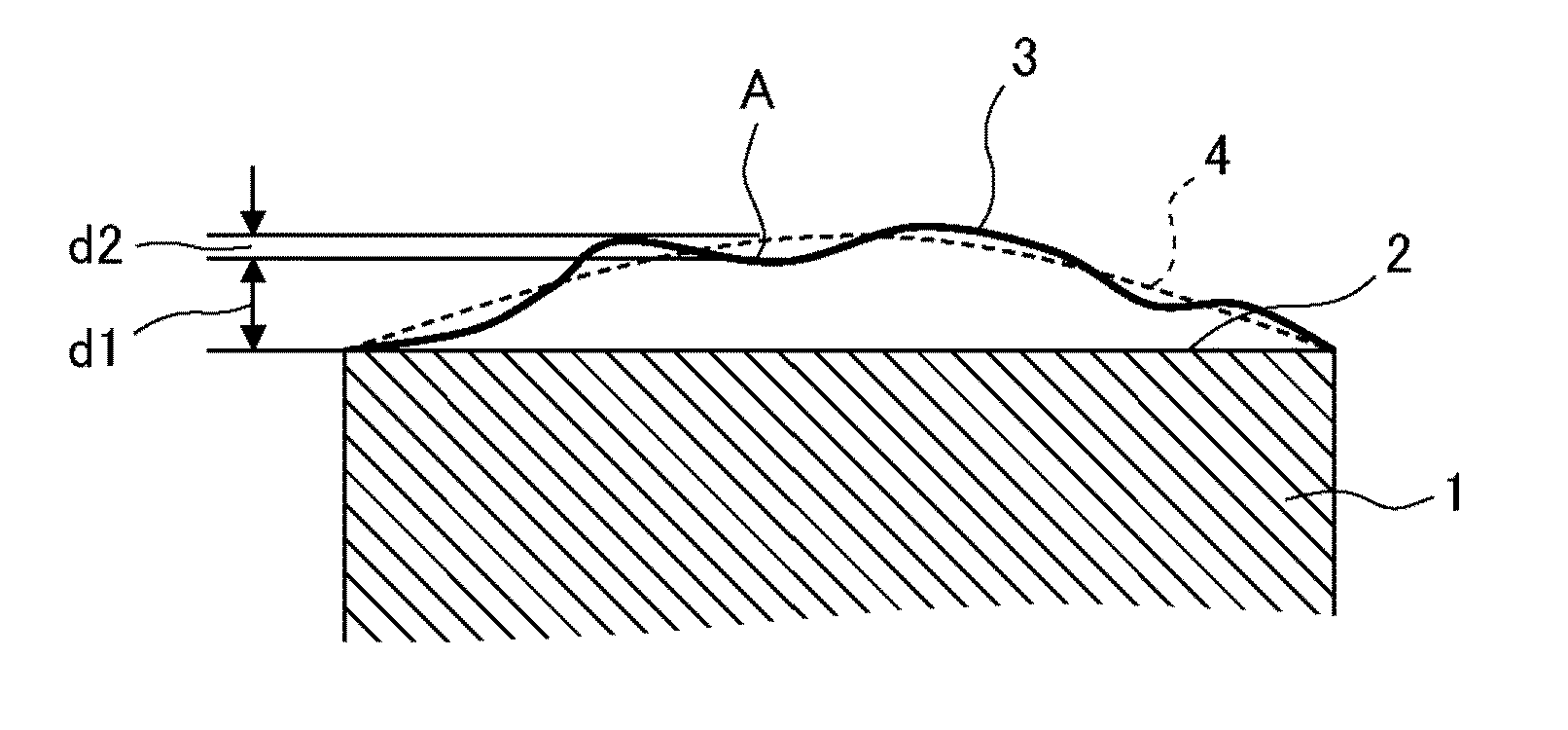
[0164]The values of the mechanical flatness of Samples A and B in Examples were, as represented by TIR (Total Indicator Reading) which is a sum of absolute value of highest point and absolute value of lowest point, 216 nm and 249 nm respectively in the case of 146 mm×146 mm region. In the case of 132 mm×132 mm region within which a transfer exposure region (shot region) fits, the values were 138 nm and 148 nm respectively, both being 200 nm or less. Further, the values were 55 nm and 46 nm respectively in the case of a circular region of 104 mm diameter. The minimum value of the mechanical flatness of the two samples is 46 nm in the case of a circular region of 104 mm diameter, which was approximately twice the value 25 nm (rounded up to whole number) which is λ / 8 of exposure wavelength λ (193 nm) of ArF exposure.

[0165]On the other hand, in view of the optical flatness of this invention calculated by the difference shape (difference data) between the virtual reference surface and th...

reference example 1

[0173]The mechanical flatness of Sample C of Reference Examples was, as represented by TIR, 346 nm in the case of 146 mm×146 mm region; 281 nm in the case of 132 mm×132 mm region; and 81 nm in the case of a circular region of 104 mm diameter. The values are the greatest among the eight samples. Particularly in 132 mm×132 mm region within which a transfer exposure region (shot region) fits, the value was beyond 200 nm (0.2 μm). On the other hand, the optical flatness in this invention calculated by difference shape between the virtual reference surface and the principal surface actually measured in a circular region of 104 mm diameter was 13 nm as represented by PV value, the value being extremely favorable which is approximately half of 25 nm which is λ / 8 of exposure wavelength λ of ArF exposure. A mask was manufactured using this mask blank substrate and transfer evaluation was made using a scanner, resulting in excellent focus latitude, positional displacement, and resolution simi...

reference example 2

[0174]The mechanical flatness of Sample X2 of Reference Examples was, in TIR, 126 nm in the case of 146 mm×146 mm region; 81 nm in the case of 132 mm×132 mm region; and 29 nm in the case of a circular region of 104 mm diameter. These are small values as in Sample X1 of Comparative Examples. On the other hand, the optical flatness of this invention calculated by the difference shape between the virtual reference surface and the principal surface actually measured in the circular region of 104 mm diameter was 19 nm in PV value, which was a favorable value of 25 nm or less which is λ / 8 of exposure wavelength λ of ArF exposure. However, the determination coefficient R2 was as small as 0.637, and divergence in fitting with the optically flat surface (virtual reference surface) in the entire circular region of 104 mm diameter was conspicuous.

[Manufacture of Mask Blank]

[0175]An example of the manufacture of a halftone type mask blank is given below. First, mask blank substrates manufacture...


PUM

PropertyMeasurementUnit
diameteraaaaaaaaaa
diameteraaaaaaaaaa
flatnessaaaaaaaaaa

Abstract

Provided are a mask blank substrate which has effectively and extremely high principal surface flatness while a reduction in the manufacturing throughput of the mask blank substrate is suppressed, a mask blank, and a transfer mask. Also provided are manufacturing methods therefor.A virtual reference surface that becomes an optically effective flat reference surface defined by a Zernike polynomial which is composed of only terms in which the order of a variable related to a radius is the second or lower order, and includes one or more terms in which the order of the variable related to the radius is the second order is set, and a mask blank substrate satisfying the condition that data (PV value) relating to the difference between the maximum value and the minimum value of the difference data between the reference surface and the measured shape of the mask blank substrate is one-eighth or less of an exposure wavelength (A) is selected.

Description

TECHNICAL FIELD[0001]This invention relates to a mask blank substrate, a mask blank, and a mask for use in photolithography, and manufacturing methods therefor, and a manufacturing method of a semiconductor device, particularly, a mask blank substrate, a mask blank, a mask, and methods of manufacturing therefor, and a method of manufacturing a semiconductor device that are preferable in securing a focus latitude when photolithography is conducted.BACKGROUND ART[0002]An increase in NA (high numerical aperture) of exposure apparatus using ArF exposure light of 193 nm wavelength is in progress to deal with the miniaturization of semiconductor devices. A further increase in NA has been made as a result of the introduction of a liquid immersion exposure technique, presently leading to the practical application of NA 1.35.[0003]To deal with such demands for miniaturization and increases in NA, higher flatness of a transfer mask is expected. When the flatness of a mask surface as an object...

Claims


Application Information

Patent Timeline
Patent Type & Authority Applications(United States)
IPC IPC(8): G03F1/50H01L21/027G03F7/20
CPCG03F1/50H01L21/0274G03F7/20C03C15/02C03C17/22G03F1/60
Inventor TANABE, MASARU
Owner HOYA CORP
Why Eureka
Try Eureka