Micro/nano imprint mold of the fabricating process

a technology of micro-nano imprinting and fabricating process, which is applied in the field of micro-nano imprinting mold of fabricating process, can solve the problems of high prior art lithography etching cost, high cost of photoresist with high resolution, and difficulty in meeting the needs of different etching process, etc., and achieves the effect of low cos

Inactive Publication Date: 2014-03-04
NAT TAIWAN UNIV OF SCI & TECH
View PDF14 Cites 0 Cited by
  • Summary
  • Abstract
  • Description
  • Claims
  • Application Information

AI Technical Summary

Benefits of technology

[0011]Accordingly, a scope of the invention is to provide a micro/nano imprint mold of the fabricating pro

Problems solved by technology

(1) The photoresist with high resolution is expensive.
The price of photoresist can be reach hundreds of thousands of US Dollars per liter so that the cost of the lithography etching process is high in prior art.
Additionally, because the less selection of the material, it is difficult to meet the need of the different etching process.
For example, the anti-etching ability of the photoresist of the PMMA is poor.
Using the aligner exposure machine to expose all substrate is fast, but the resolution of the lithography etching process is limited (line width shall be larger than 2 μm).
So that the photoresist with low anti-etching ability and thin-film thickness shall be used, the etching structure with high aspect ratio is difficult to fabricate.
(3)

Method used


Image

  • Micro/nano imprint mold of the fabricating process
  • Micro/nano imprint mold of the fabricating process
  • Micro/nano imprint mold of the fabricating process

Examples


Embodiment Construction

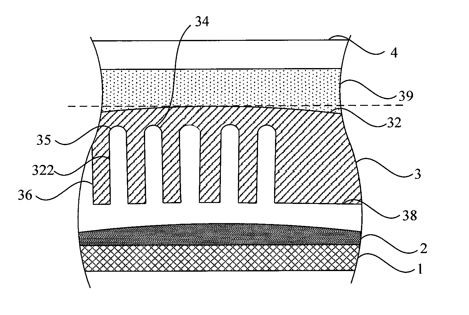
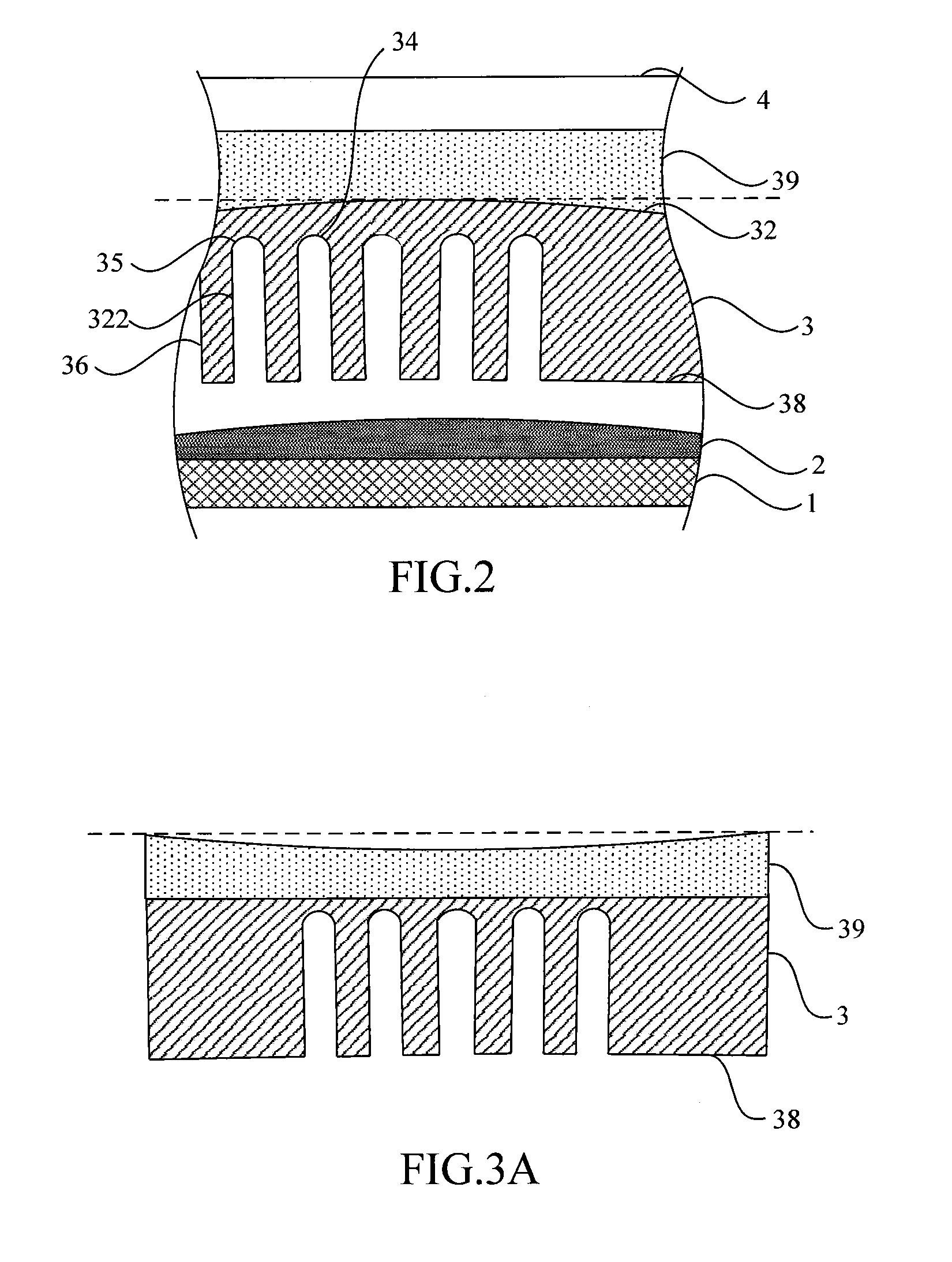
[0030]Please refer to FIG. 2. FIG. 2 illustrates a schematic diagram of the micro / nano imprint mold of the fabricating process according to an embodiment of the invention. The invention is to provide a mold 3 for the micro / nano imprint fabricating process for imprinting a pattern to a substrate 1 by a material layer 2. The mold 3 comprises an upper surface 32, a lower surface 34, a pre-determined structure 36 and an overflow controlling device 38. The upper surface 32 is corresponded to the lower surface 34. The pre-determined structure 36 is disposed on the lower surface 34 of the mold 3. The overflow controlling device 38 is used to maintain the pressure of the material layer 2 between the mold 3 and the substrate 1. Furthermore, the upper surface 32 of the mold 3 faces a pressing plate 4. The pressing plate 4 is connected to a power source to drive and provide energy to the mold 3.

[0031]In the embodiment, the substrate 1 is made of sapphire for fabricating the light emitting diod...


PUM

PropertyMeasurementUnit
Thicknessaaaaaaaaaa
Pressureaaaaaaaaaa
Flexibilityaaaaaaaaaa

Abstract

The invention discloses a mold performing in the micro/nano imprint fabricating process, wherein the mold is utilized to imprint a pattern on a substrate via a material layer. The mold comprises an upper surface, a lower surface, a pre-determined structure and an overflow controlling device. The upper surface and the lower surface are corresponded to each other. The pre-determined structure is disposed on the lower surface of the mold. The overflow controlling device is utilized to maintain the pressure among the material layer and the substrate.

Description

CROSS-REFERENCE TO RELATED APPLICATION[0001]This application claims priority based on Taiwanese Patent Application No. 099139717, filed on Nov. 18, 2010, the disclosure of which is incorporated herein by reference in its entirety.BACKGROUND OF THE INVENTION[0002]1. Field of the Invention[0003]The present invention relates to a micro / nano imprint mold of the fabricating process and the method of fabricating etching barrier pattern or anti-etch structure with high aspect ratio by utilizing thereof. More particularly, the present invention relates to a mold and the method thereof which are used to improve the accuracy of fabricated pattern and the pressure distribution among the substrate.[0004]2. Description of the Prior Art[0005]Light-emitting diode (LED) wafers will become epitaxial wafers by a fabricating process. The epitaxial wafers fabricating process comprises a MOCVD process. The growth of the materials is horizontally stacked, the defection rate of the lattice is low and the ...

Claims


Application Information

Patent Timeline
IPC IPC(8): B29C59/02
CPCB82Y40/00B82Y10/00G03F7/0002
Inventor CHANG, FUH-YU
Owner NAT TAIWAN UNIV OF SCI & TECH
Why Eureka
Try Eureka