Light-Emitting Device, Module, Electronic Device, and Method for Manufacturing Light-Emitting Device

a technology of light-emitting devices and electronic devices, which is applied in the direction of thermoelectric devices, sustainable manufacturing/processing, and final product manufacturing, etc., can solve problems such as erode reliability, and achieve the effect of high reliability and high reliability

Active Publication Date: 2016-04-21
SEMICON ENERGY LAB CO LTD
View PDF10 Cites 37 Cited by
  • Summary
  • Abstract
  • Description
  • Claims
  • Application Information

AI Technical Summary

Benefits of technology

[0011]An object of one embodiment of the present invention is to provide a highly reliable light-emitting device, display device, electronic device, or lighting device. Alternatively, an object of one embodiment of the present invention is to provide a highly reliable flexible light-emitting device, display device, electronic device, or lighting device.

Problems solved by technology

An organic EL element has a problem in that entry of impurities such as moisture or oxygen from the outside erodes the reliability.
This is because an organic compound or a metal material contained in the organic EL element reacts with the impurities such as moisture or oxygen and thus deteriorates.

Method used


Image

  • Light-Emitting Device, Module, Electronic Device, and Method for Manufacturing Light-Emitting Device
  • Light-Emitting Device, Module, Electronic Device, and Method for Manufacturing Light-Emitting Device
  • Light-Emitting Device, Module, Electronic Device, and Method for Manufacturing Light-Emitting Device

Examples


embodiment 1

[0092]In this embodiment, a light-emitting device of one embodiment of the present invention and a manufacturing method thereof will be described with reference to FIGS. 1A to 1D, FIGS. 2A to 2D, FIGS. 3A to 3F, FIGS. 4A to 4D, FIGS. 5A to 5E, FIGS. 6A and 6B, FIGS. 7A and 7B, FIGS. 8A to 8D, FIGS. 9A to 9D, FIGS. 10A and 10B, FIGS. 11A to 11C, FIGS. 12A to 12D, FIGS. 13A to 13D, FIGS. 14A and 14B, FIGS. 15A to 15D, FIGS. 16A to 16D, FIGS. 17A to 17C, FIGS. 18A to 18D, FIGS. 19A to 19D, FIGS. 20A to 20D, FIGS. 21A to 21D, FIGS. 22A to 22D, and FIGS. 23A1, 23A2, 23B1, 23B2, and 23C.

[0093]Although light-emitting devices including organic EL elements are mainly described as examples in this embodiment, one embodiment of the present invention is not limited to these examples. A light-emitting device or a display device including another light-emitting element or display element which will be described in Embodiment 2 as an example is also one embodiment of the present invention. Moreove...

example a-1

STRUCTURE EXAMPLE a-1

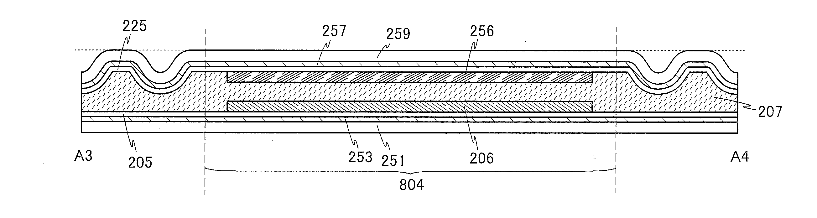
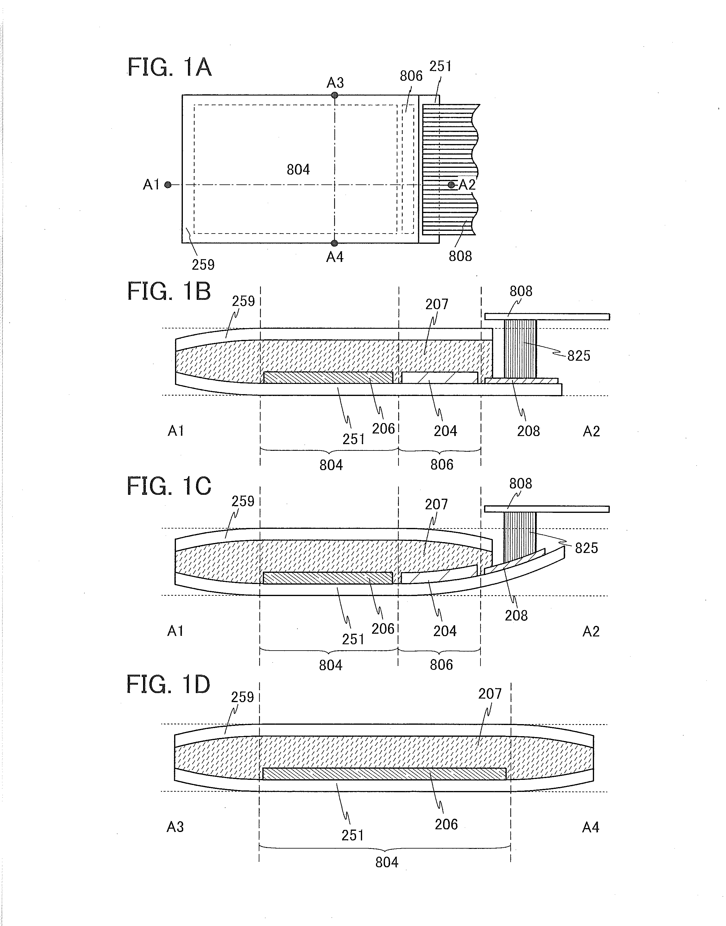
[0110]FIG. 1A is a top view of a light-emitting device. FIG. 1B is a cross-sectional view taken along a dashed-dotted line A1-A2 in FIG. 1A. FIG. 1C illustrates a modification example of FIG. 1B. FIG. 1D is a cross-sectional view taken along a dashed-dotted line A3-A4 in FIG. 1A.

[0111]The light-emitting device illustrated in FIG. 1A includes a light-emitting portion 804 and a driver circuit portion 806. Portions other than the light-emitting portion 804 in the light-emitting device can be regarded as non-light-emitting portions. In other words, the non-light-emitting portion is provided outside the light-emitting portion 804 to have a frame-like shape. For example, the driver circuit portion 806 is a non-light-emitting portion.

[0112]The light-emitting device in FIGS. 1A to 1D includes a substrate 251, a functional layer 204, a functional layer 206, a bonding layer 207, a conductive layer 208, and a substrate 259.

[0113]In the light-emitting portion 804, the funct...

example a-2

STRUCTURE EXAMPLE a-2

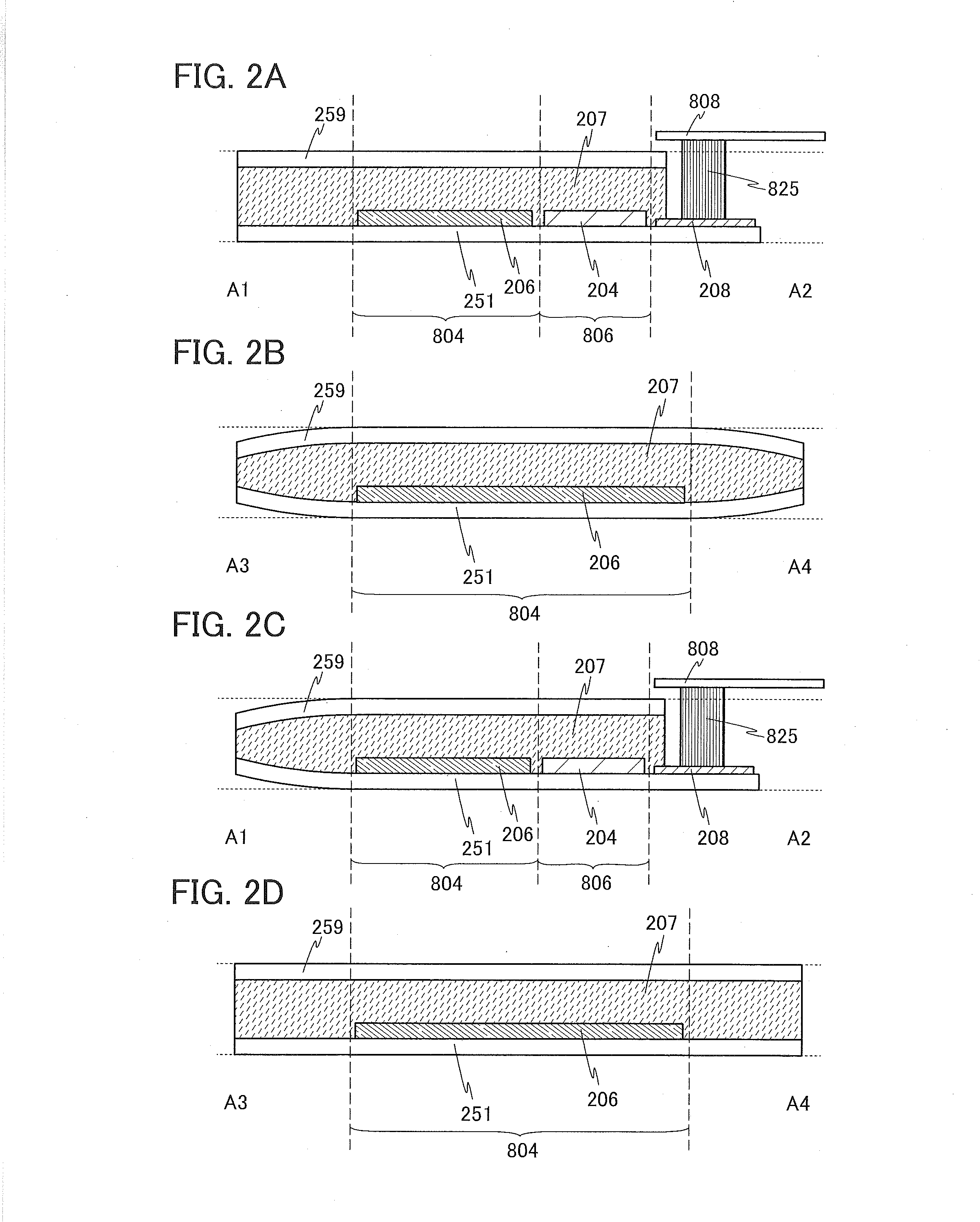
[0133]FIG. 3A is a cross-sectional view taken along the dashed-dotted line A1-A2 in FIG. 1A. FIG. 3B is a cross-sectional view taken along the dashed-dotted line A3-A4 in FIG. 1A.

[0134]The light-emitting device in FIGS. 3A and 3B includes the substrate 251, a bonding layer 253, the functional layer 204, an insulating layer 205, the functional layer 206, the bonding layer 207, the conductive layer 208, and the substrate 259.

[0135]In the light-emitting portion 804, the functional layer 206 is provided over the insulating layer 205. The substrate 251 and the insulating layer 205 are attached to each other with the bonding layer 253.

[0136]As the insulating layer 205, an insulating layer having an excellent gas barrier property, an excellent water-resistant property, an excellent moisture-resistant property, or the like is preferably used.

[0137]As an insulating layer having an excellent moisture-resistant property, a film containing nitrogen and silicon (e.g., a sili...


PUM


Abstract

A light-emitting element, a bonding layer, and a frame-like partition are formed over a substrate. The partition is provided to surround the bonding layer and the light-emitting element, with a gap left between the partition and the bonding layer. A pair of substrates overlap with each other under a reduced-pressure atmosphere and then exposed to an air atmosphere or a pressurized atmosphere, whereby the reduced-pressure state of a space surrounded by the pair of substrates and the partition is maintained and atmospheric pressure is applied to the pair of substrates. Alternatively, a light-emitting element and a bonding layer are formed over a substrate. A pair of substrates overlap with each other, and then, pressure is applied to the bonding layer with the use of a member having a projection before or at the same time as curing of the bonding layer.

Description

TECHNICAL FIELD[0001]One embodiment of the present invention relates to a light-emitting device, a module, an electronic device, and a manufacturing method thereof. In particular, one embodiment of the present invention relates to a light-emitting device utilizing organic electroluminescence (EL), and a manufacturing method thereof.[0002]Note that one embodiment of the present invention is not limited to the above technical field. Examples of the technical field of one embodiment of the present invention include a semiconductor device, a display device, a light-emitting device, a power storage device, a memory device, an electronic device, a lighting device, an input device (e.g., a touch sensor), an input-output device (e.g., a touch panel), a driving method thereof, and a manufacturing method thereof.BACKGROUND ART[0003]Recent light-emitting devices and display devices are expected to be applied to a variety of uses and become diversified.[0004]For example, light-emitting devices ...

Claims


Application Information

Patent Timeline
Patent Type & Authority Applications(United States)
IPC IPC(8): H01L27/32H01L51/56H01L51/52
CPCH01L27/3276H01L27/3262H01L51/5246H01L2227/323H01L51/56H01L2251/5338H01L27/322Y02E10/549Y02P70/50H10K77/111H10K50/8426H10K2102/351H10K59/131H10K71/00H10K59/1213H10K59/38H10K59/1201H10K2102/311
Inventor CHIDA, AKIHIRO
Owner SEMICON ENERGY LAB CO LTD
Why Eureka
Try Eureka