Resistive random access memory
a random access and memory technology, applied in the field of resistive random access memory, can solve the problems of reducing volume and difficulty in and achieve the effect of increasing the integration density of memory modules
- Summary
- Abstract
- Description
- Claims
- Application Information
AI Technical Summary
Benefits of technology
Problems solved by technology
Method used
Image
Examples
Embodiment Construction
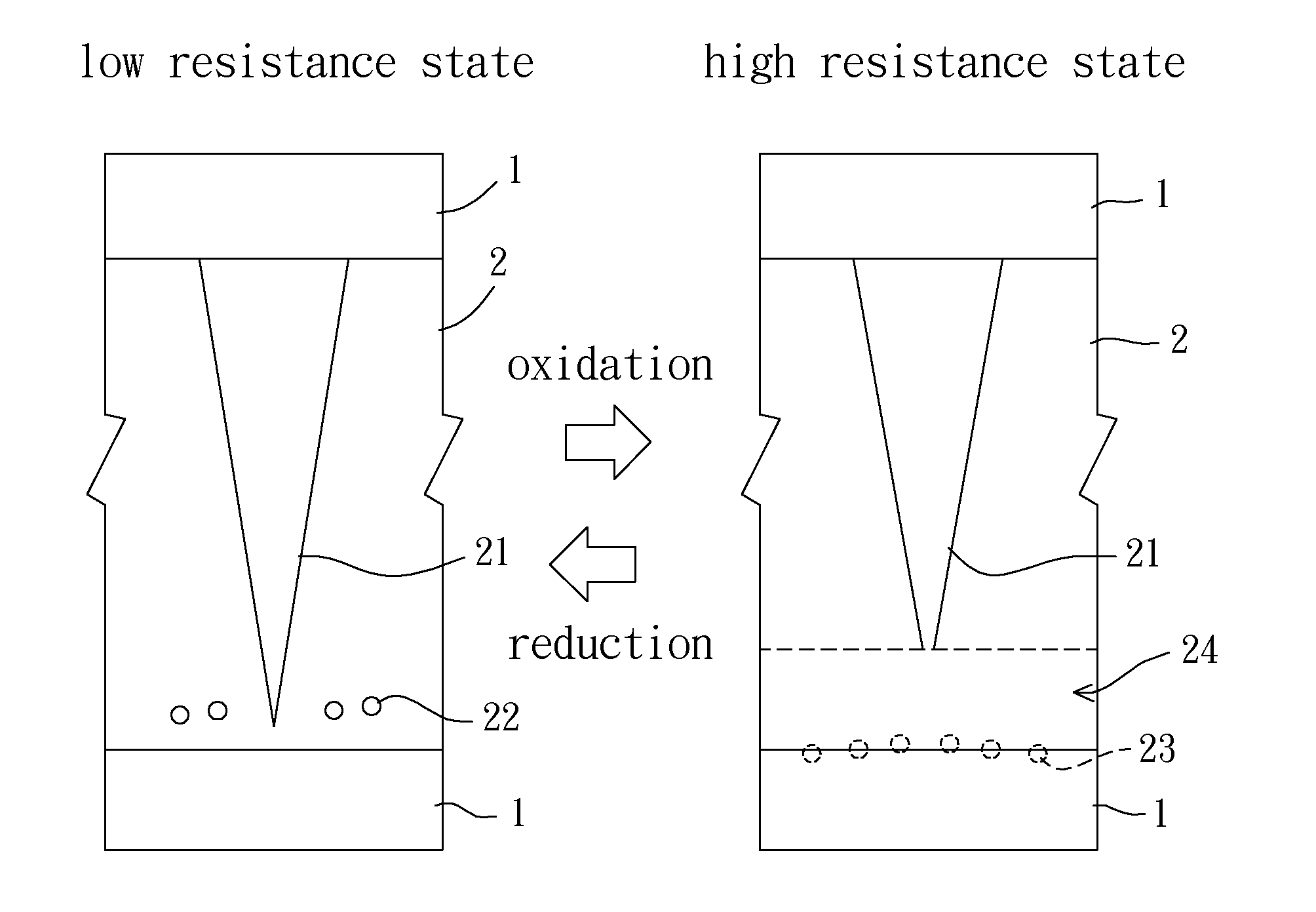
[0030]FIG. 2 is a perspective view of a resistive random access memory of an embodiment according to the present invention. The resistive random access memory includes two electrode layers 1 and a multi-resistance layer 2. The electrode layers 1 are made of a conductive material and are used to apply a working signal to the resistive random access memory. The multi-resistance layer 2 is mounted between the two electrode layers 1. The multi-resistance layer 2 consists essentially of insulating material with oxygen and lithium ions and is used to generate multi-resistance states, such as a first low resistance state (first LRS), a second low resistance state (second LRS), a first high resistance state (first HRS), and a second high resistance state (second HRS). However, the present invention is not limited to this example. The resistive random access memory can be formed by, but not limited to, a conventional sputtering procedure for forming semiconductors to reduce the manufacturing...
PUM
 Abstract
Description
Claims
Application Information


