Method And System For Silicon Photonics Wavelength Division Multiplexing Transceivers

a wavelength division multiplexing and transceiver technology, applied in the field of silicon photonics, can solve the problems of cable bulk penalties, large power requirements, and complex structure, and achieve only modest improvements in reach and limited scalability

Inactive Publication Date: 2016-04-28
CISCO TECH INC
View PDF3 Cites 76 Cited by
  • Summary
  • Abstract
  • Description
  • Claims
  • Application Information

AI Technical Summary

Benefits of technology

[0005]A system and/or method for silicon photonics wavelength division multiplexing transceivers, substantially as shown in and/or described in connection with at least one of the figures, as set forth more completely in

Problems solved by technology

They can be mitigated to some extent with equalization, coding, and shielding, but these techniques require considerable

Method used


Image

  • Method And System For Silicon Photonics Wavelength Division Multiplexing Transceivers
  • Method And System For Silicon Photonics Wavelength Division Multiplexing Transceivers
  • Method And System For Silicon Photonics Wavelength Division Multiplexing Transceivers

Examples


Embodiment Construction

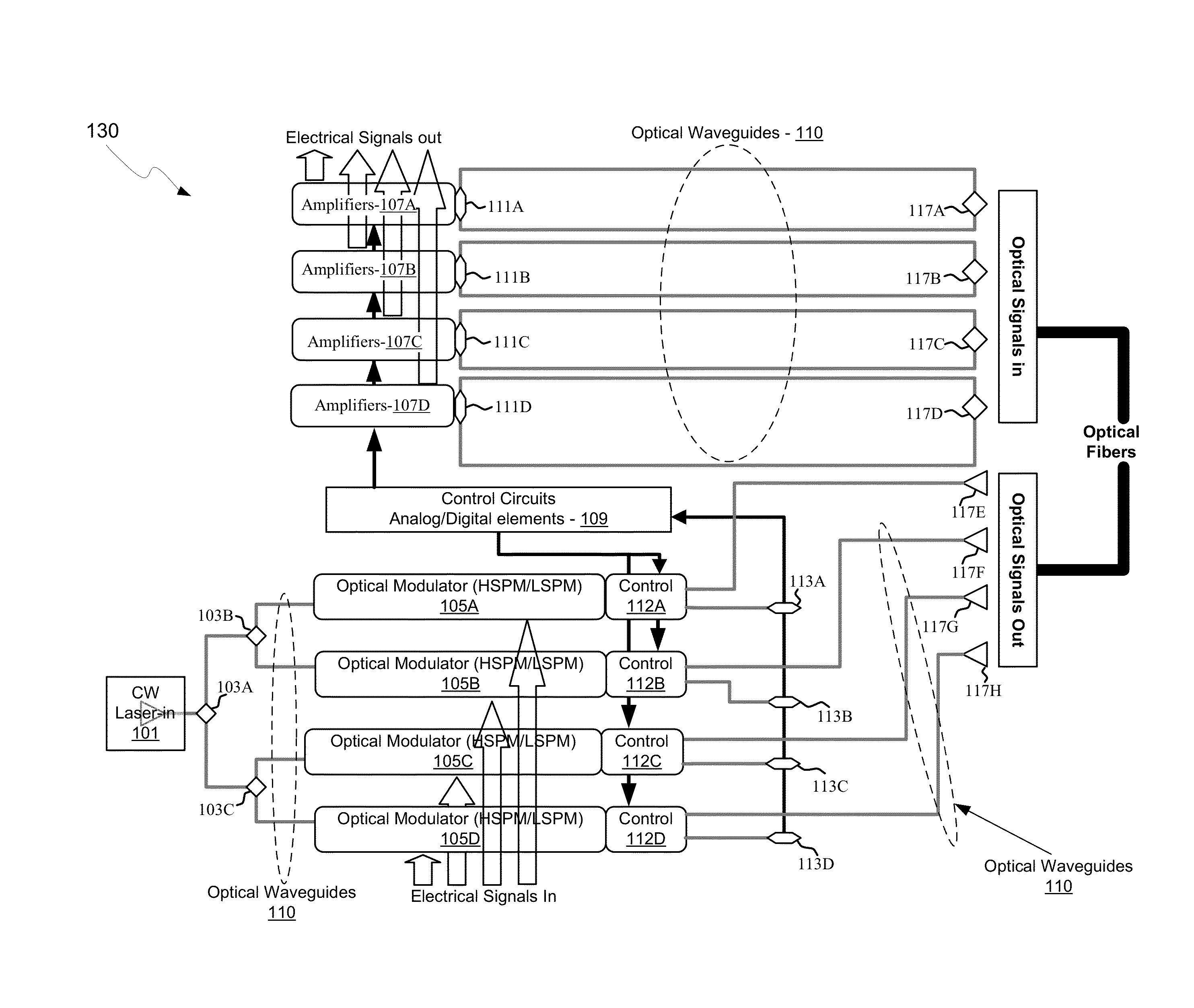
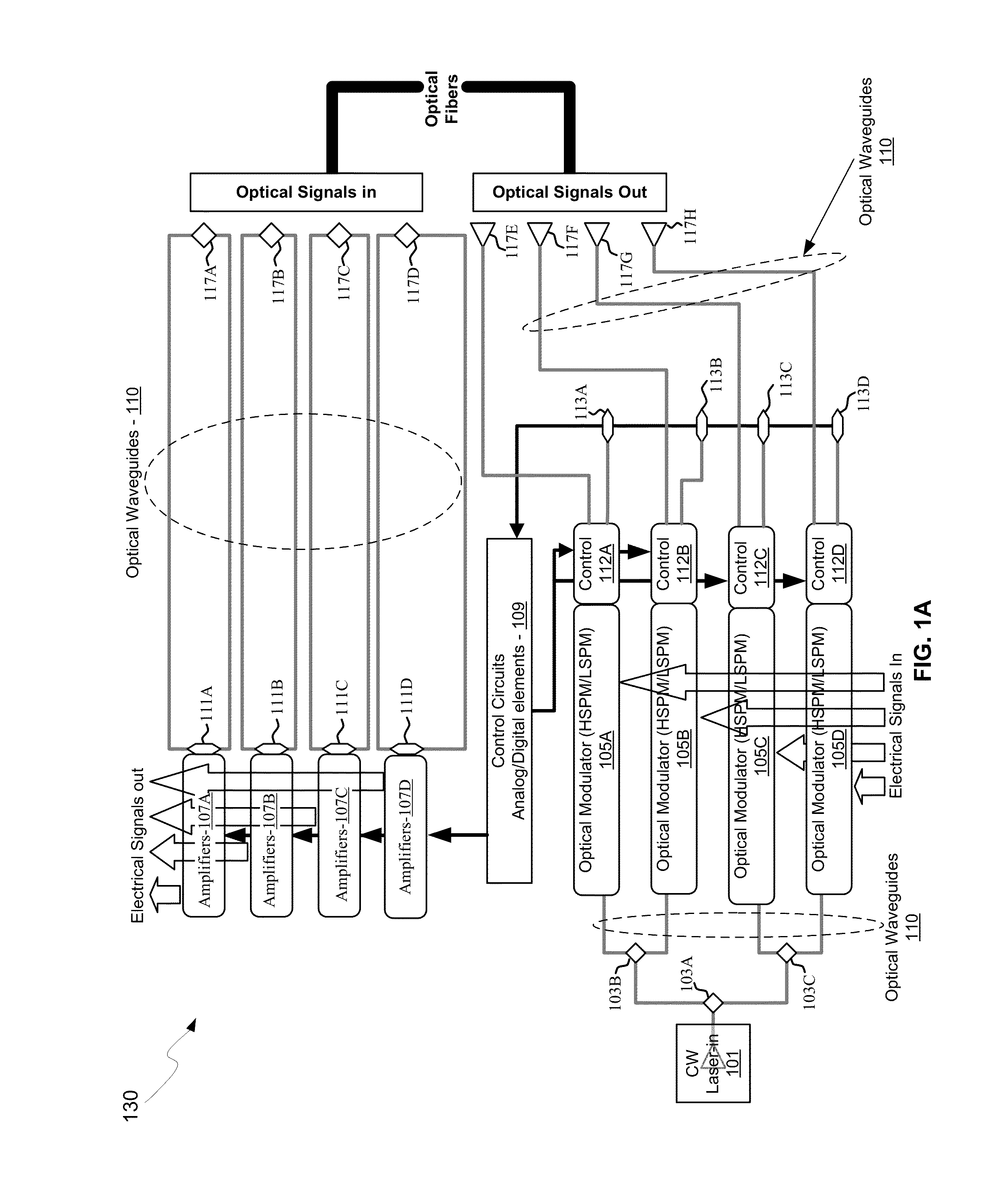
[0027]Certain aspects of the disclosure may be found in a method and system for silicon photonics wavelength division multiplexing transceivers. Exemplary aspects of the disclosure may comprise, in a transceiver integrated in a silicon photonics chip: generating a first modulated output optical signal at a first wavelength utilizing a first electrical signal, generating a second modulated output optical signal at a second wavelength utilizing a second electrical signal, and communicating the first and second modulated output optical signals into an optical fiber coupled to the chip utilizing a multiplexing grating coupler in the chip. A received input optical signal may be split into a modulated input optical signal at the first wavelength and a modulated input optical signal at the second wavelength utilizing a demultiplexing grating coupler in the chip. The modulated input optical signal at the first wavelength may be converted to a first electrical input signal utilizing a first ...


PUM


Abstract

Methods and systems for silicon photonics wavelength division multiplexing transceivers are disclosed and may include, in a transceiver integrated in a silicon photonics chip: generating a first modulated output optical signal at a first wavelength utilizing a first electrical signal, generating a second modulated output optical signal at a second wavelength utilizing a second electrical signal, communicating the first and second modulated output optical signals into an optical fiber coupled to the chip utilizing a multiplexing grating coupler in the chip. A received input optical signal may be split into a modulated input optical signal at the first wavelength and a modulated input optical signal at the second wavelength utilizing a demultiplexing grating coupler in the chip. The first and second modulated input optical signals may be converted to first and second electrical input signals utilizing first and second photodetectors in the chip.

Description

CROSS-REFERENCE TO RELATED APPLICATIONS / INCORPORATION BY REFERENCE[0001]This application claims priority to and the benefit of U.S. Provisional Application 62 / 122,718 filed on Oct. 28, 2014, which is hereby incorporated herein by reference in its entirety.FIELD[0002]Certain embodiments of the disclosure relate to semiconductor photonics. More specifically, certain embodiments of the disclosure relate to a method and system for silicon photonics wavelength division multiplexing transceivers.BACKGROUND[0003]As data networks scale to meet ever-increasing bandwidth requirements, the shortcomings of copper data channels are becoming apparent. Signal attenuation and crosstalk due to radiated electromagnetic energy are the main impediments encountered by designers of such systems. They can be mitigated to some extent with equalization, coding, and shielding, but these techniques require considerable power, complexity, and cable bulk penalties while offering only modest improvements in reac...

Claims


Application Information

Patent Timeline
IPC IPC(8): H04B10/25H04B10/516
CPCH04B10/516H04B10/2504H04B10/40H04B10/506H04B10/5053H04J14/02
Inventor MEKIS, ATTILADE DOBBELAERE, PETERVERSLEGERS, LIEVENSUN, PENGDE KONINCK, YANNICK
Owner CISCO TECH INC
Why Eureka
Try Eureka