Display panel, display device and manufacturing method thereof

a technology for display panels and display devices, applied in the field of display panels, can solve the problems of reducing reflection, ar film can only achieve a zero reflection within a narrow wavelength range, and cannot eliminate all the reflected light with wavelength of visible light, so as to improve image quality and product quality, the effect of increasing the thickness of the display panel

Active Publication Date: 2016-05-05
BOE TECH GRP CO LTD
View PDF5 Cites 7 Cited by
  • Summary
  • Abstract
  • Description
  • Claims
  • Application Information

AI Technical Summary

Benefits of technology

[0007]The embodiments of the present invention provide a display panel, a method for manufacturing the display panel, a display device, and a method for manufacturing the display device, thereby solving the problem that attaching an AR film can only achieve a zero reflection within a narrow wavelength range.
[0017]employing the black matrix as a mask plate; exposing the photoresist from a side of the first surface of the base substrate, such that the photoresist corresponding to the position of the display units is cured.
[0036]employing the black matrix as a mask plate; exposing the photoresist from a side of the first surface of the base substrate, such that the photoresist corresponding to the position of the display units is cured.
[0040]The embodiments of the present invention provide a display panel, a method for manufacturing the display panel, a display device, and a method for manufacturing the display device. The method for manufacturing a display panel comprises: firstly, forming a black matrix on a first surface of a base substrate, and defining a plurality of display units with the criss-cross black matrix; then forming a photoresist on a second surface of the base substrate, wherein the first surface is arranged opposite to the second surface; since the display area of the display panel corresponds to the position of the display units, then performing a curing process for the photoresist corresponding to the position of the display units, such that the portion of the base substrate corresponding to the position of the display units can be protected; then removing the photoresist corresponding to the position of the black matrix, such that the portion of the second surface of the base substrate corresponding to the position of the black matrix is not covered by the photoresist; then, performing a texturing process for a portion of the second surface of the base substrate corresponding to the position of the black matrix, such that this portion is coarse. In such a manner, when visible light is incident to the non display area of the display panel corresponding to the black matrix, diffuse reflection will occur for all visible light incident to the non display area due to the coarse surface, which can eliminate the reflected light in the non display area. Although etching process is not performed for the portion of the base substrate corresponding to the position of the display area, the reflected light in the display area has little influence on the display effect, since the intensity of the light emitted from the display area (for display) is far greater than the intensity of the reflected light. Therefore, on the premise of ensuring the normal display of the display panel, the embodiment provided by the present invention eliminates the reflected light of all the visible light incident to the non display area, without increasing the thickness of the display panel, thereby improving the image quality and product quality.

Problems solved by technology

In such a manner, for light incident to the AR film from a same point, a coherent addition will be performed for two reflected light beams, one of these reflected light beams being reflected at the interface between air and the AR film 14, the other being reflected at the interface between the AR film 14 and the surface of the polarizer 13, resulting in a destructive interference, thereby reducing the reflection.
Therefore, the AR film can only achieve a zero reflection within a narrow wavelength range, and can not eliminate all the reflected light with wavelength of the visible light.

Method used


Image

  • Display panel, display device and manufacturing method thereof
  • Display panel, display device and manufacturing method thereof
  • Display panel, display device and manufacturing method thereof

Examples


embodiment 1

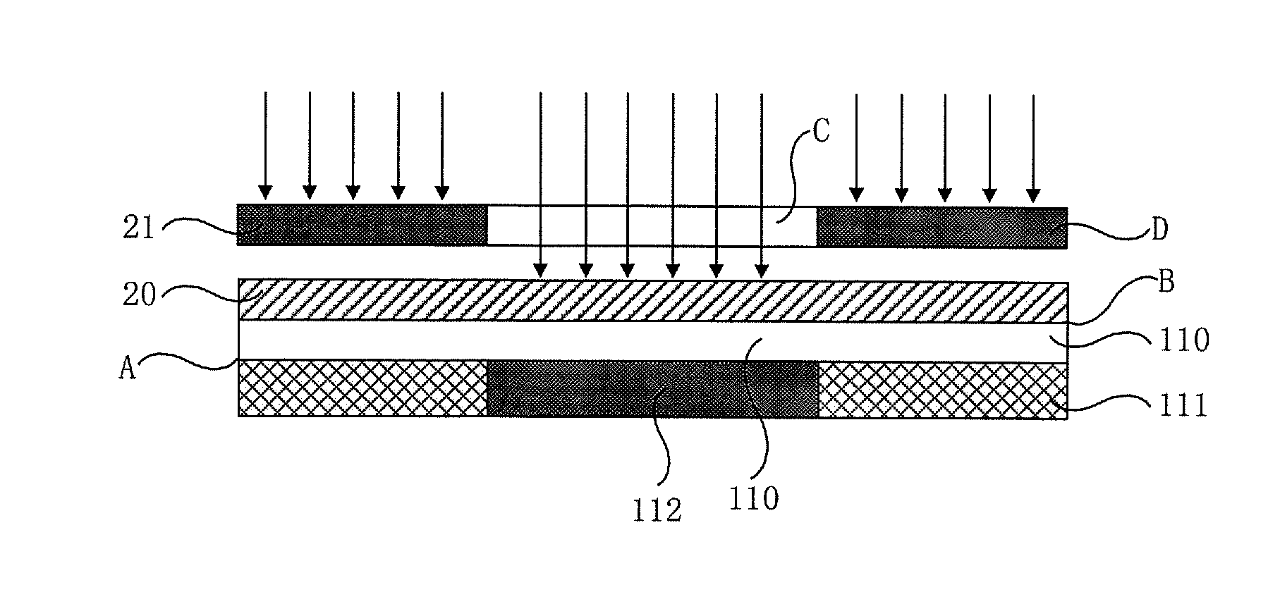
[0077]S201, after the above mentioned step S101, as shown in FIG. 4 and FIG. 5a, providing a mask plate 21 on the surface of the photoresist 20, a transparent area C of the mask plate 21 being corresponding to the position of the display units 112, and an opaque area D of the mask plate 21 being corresponding to the position of the black matrix 111.

[0078]S202, exposing the photoresist 20 such that the photoresist 20 corresponding to the transparent area C of the mask plate 21 is cured, therefore the portion of the surface of the base substrate 110 corresponding to the display area is protected from being roughened by the texturing process.

[0079]S203, if the base substrate 110 is a glass substrate, dry air can be filled into the hydrofluoric acid solution to form an etching solution with bubbles. Moreover, as shown in FIG. 5b, the etching solution 22 can be sprayed on the second surface B of the base substrate 110 with a high pressure gas, forming a coarse surface as shown in FIG. 3d...

embodiment 2

[0082]After the above mentioned step 5101, as shown in FIG. 6, employing the black matrix 111 as a mask plate; exposing the photoresist 20 from a side of the first surface A of the base substrate 110, such that the photoresist 20 corresponding to the position of the display units 112 is cured, therefore the portion of the surface of the base substrate 110 corresponding to the display area is protected from being roughened by the texturing process.

[0083]Then, the step S203 and S204, or the step S104 can be carried out.

[0084]Compared with the embodiment 1, the embodiment 2 uses the opaque characteristic of the black matrix 111, exposuring in a different direction, omitting the step of providing the mask plate 21.

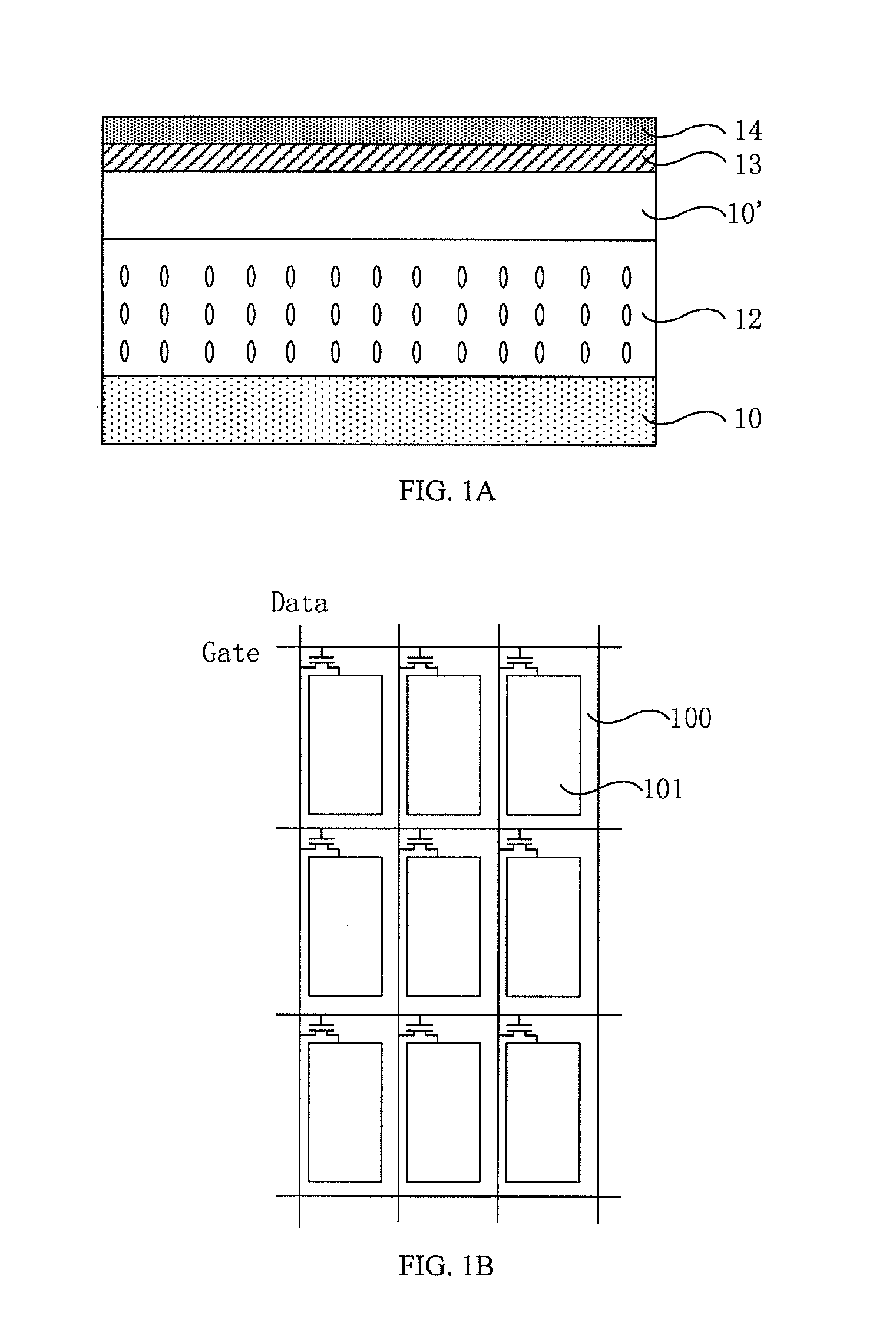
[0085]An embodiment of the present invention provides a display substrate, as shown in FIG. 3d, wherein the display substrate comprises a base substrate 110, a black matrix 111 on a first surface A of the base substrate 110, and a plurality of display units 112 defined with th...

embodiment 3

[0095]S401, after the above mentioned step 5301, as shown in FIG. 9 and FIG. 10, providing a mask plate 21 on the surface of the photoresist 20, a transparent area C of the mask plate 21 being corresponding to the position of the display units 112, and an opaque area D of the mask plate 21 being corresponding to the position of the black matrix 111.

[0096]S402, exposing the photoresist 20 such that the photoresist 20 corresponding to the transparent area C of the mask plate 21 is cured, therefore the portion of the surface of the base substrate 110 corresponding to the display area is protected from being roughened by the texturing process.

[0097]S403, if the base substrate 110 is a glass substrate, dry air can be filled into the hydrofluoric acid solution to form an etching solution with bubbles. Moreover, as shown in FIG. 5b, the etching solution 22 can be sprayed on a surface of the base substrate 110 departing from the array substrate 10 (i.e., the second surface B) with a high pr...


PUM

PropertyMeasurementUnit
transparentaaaaaaaaaa
areaaaaaaaaaaa
volumeaaaaaaaaaa

Abstract

The embodiments of the present invention provide a display panel, a method for manufacturing the display panel, a display device, and a method for manufacturing the display device, relating to the technical field of display, thereby solving the problem that the anti-reflection effect of AR film is poor, since attaching an AR film can only achieve a zero reflection within a narrow wavelength range. The method for manufacturing a display panel comprises forming a black matrix on a first surface of a base substrate, and defining a plurality of display units with the criss-cross black matrix; forming a photoresist on a second surface of the base substrate; performing a curing process for the photoresist corresponding to the position of the display units; removing the photoresist corresponding to the position of the black matrix; and performing a texturing process for a portion of the second surface of the base substrate corresponding to the position of the black matrix.

Description

RELATED APPLICATIONS[0001]The present application claims the benefit of Chinese Patent Application No. 201410599115.7, filed Oct. 30, 2014, the entire disclosure of which is incorporated herein by reference.FIELD OF THE INVENTION[0002]The present invention relates to the technical field of display, in particular to a display panel, a method for manufacturing the display panel, a display device, and a method for manufacturing the display device.BACKGROUND OF THE INVENTION[0003]TFT-LCD (Thin Film Transistor Liquid Crystal Display) is a flat panel display, and is applied in high performance display fields increasingly because of its characteristics such as small volume, low power consumption, no radiation and the relatively low production cost.[0004]As shown in FIG. 1a, a TFT-LCD consists of an array substrate 10 and a color film substrate 10′. A liquid crystal layer 12 is arranged between the array substrate 10 and the color film substrate 10′. In addition, the upper surface of the co...

Claims


Application Information

Patent Timeline
Patent Type & Authority Applications(United States)
IPC IPC(8): G02F1/1335
CPCG02F1/133512G02F1/133502
Inventor WU, YANBING
Owner BOE TECH GRP CO LTD
Why Eureka
Try Eureka