Fin shape structure

a technology of fin and shape, applied in the field of fin shape structure, can solve the problems of many challenges and limitations of the current use of silicon material, and achieve the effects of improving the short channel effect, and reducing the cost of silicon material

Active Publication Date: 2016-05-19
MARLIN SEMICON LTD
View PDF5 Cites 19 Cited by
  • Summary
  • Abstract
  • Description
  • Claims
  • Application Information

AI Technical Summary

Benefits of technology

[0009]In the method of the present invention, a greater band offset is sufficiently provided through selectively forming the epitaxial buffer layers and the epitaxial channel layers in the fin structures respectively, such that the fin shaped structure obtained thereto can obtain SOI-like performance, and further achieve the purpose of supplying preferable channel mobility and improving the short channel effect.

Problems solved by technology

However, under the demand for continuously shrinking the size of the device, the characteristics of currently used silicon material presents many challenges and limitations.

Method used


Image

  • Fin shape structure
  • Fin shape structure
  • Fin shape structure

Examples


Embodiment Construction

[0013]In the following description, numerous specific details, as well as accompanying drawings, are given to provide a thorough understanding of the invention. It will, however, be apparent to one skilled in the art that the invention may be practiced without these specific details.

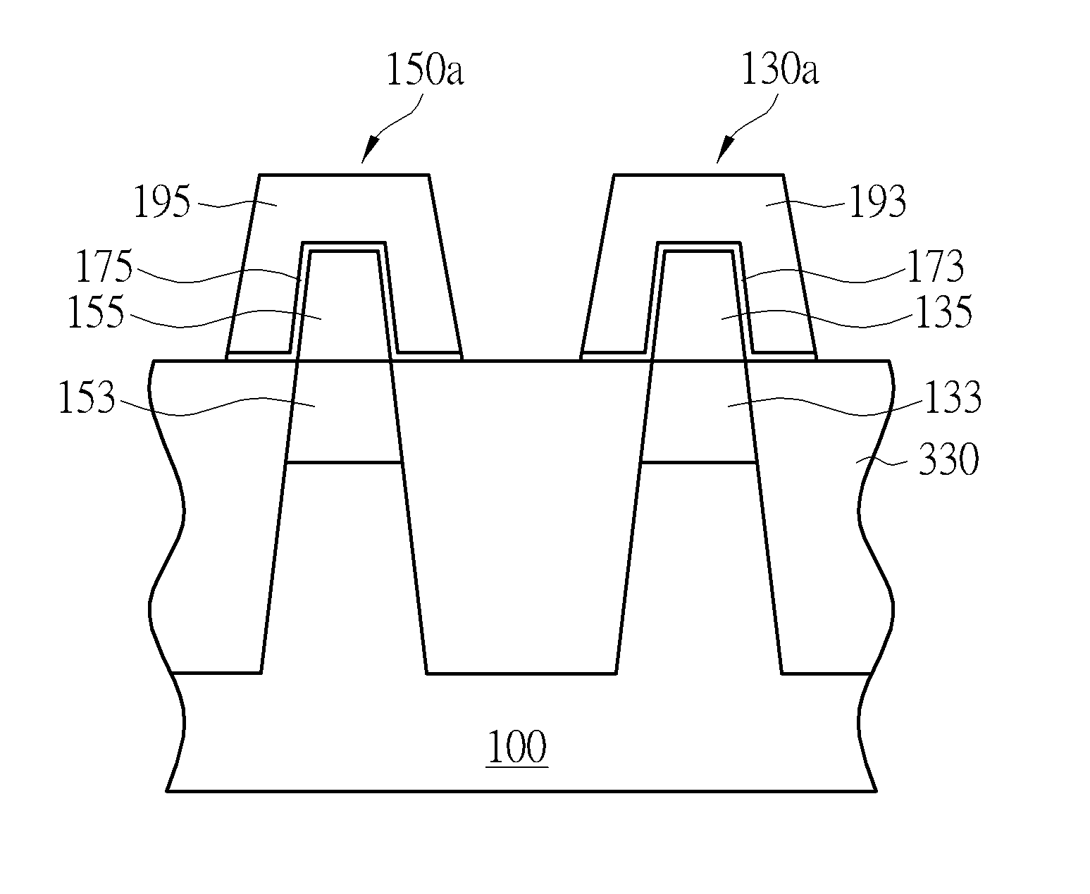
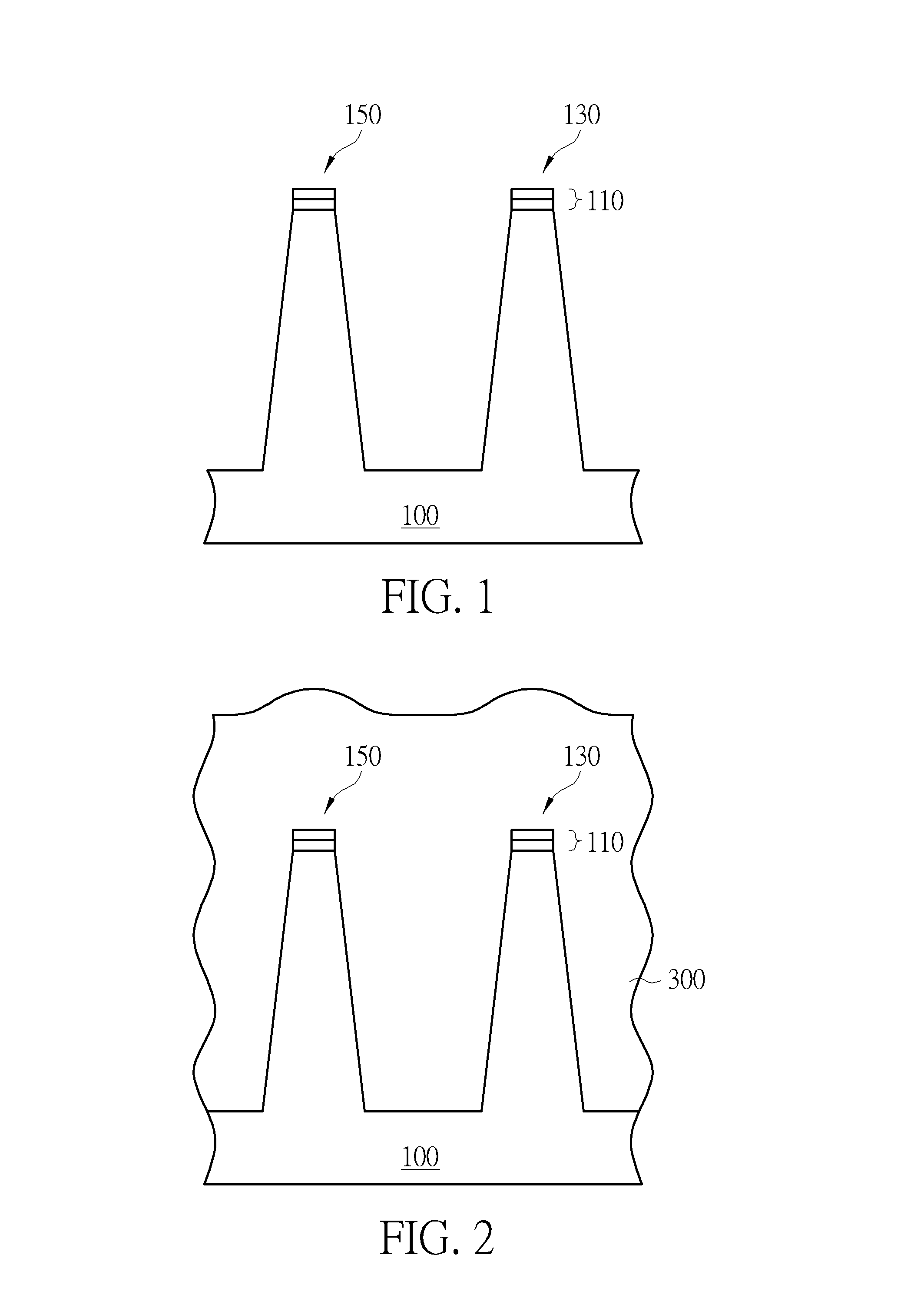
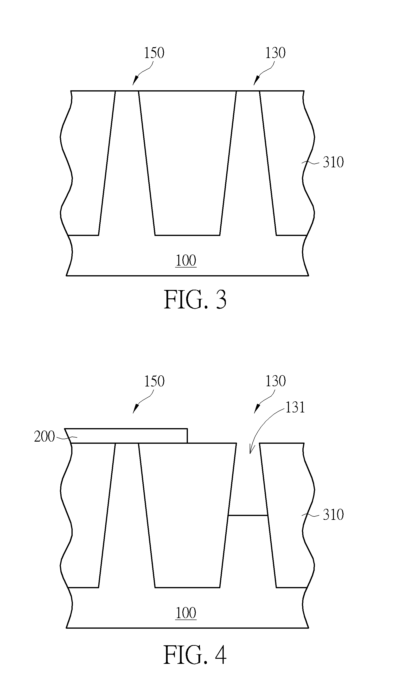
[0014]Referring to FIGS. 1-8, FIGS. 1-8 are schematic diagrams illustrating a method of forming a fin shaped structure according to a preferred embodiment of the present invention. As shown in FIG. 1, a substrate 100 is firstly provided, wherein a first fin structure 130 and a second fin structure 150 are formed on the substrate 100 respectively. The substrate 100 may include a semiconductor material, such as silicon, silicon germanium, silicon carbide, or silicon on insulator (SOI), but not limited thereto. In another embodiment, the substrate 100 may also include non-semiconductor material, such as glass. Precisely speaking, the first fin structure 130 and the second fin structure 150 may be formed by ...


PUM


Abstract

A fin shaped structure and a method of forming the same. The method includes providing a substrate having a first fin structure and a second fin structure. Next, an insulation material layer is formed on the substrate. Then, a portion of the first fin structure is removed, to form a first recess. Following this, a first buffer layer and a first channel layer are formed sequentially in the first recess. Next, a portion of the second fin structure is removed, to form a second recess. Then, a second buffer layer and a second channel layer are formed in the second recess sequentially, wherein the second buffer layer is different from the first buffer layer.

Description

BACKGROUND OF THE INVENTION[0001]1. Field of the Invention[0002]The present invention relates to a fin shaped structure and a method of forming the same, and more particularly to a fin shaped structure having a buffer layer with a band gap thereof being greater than that of a channel layer, and a method of forming the same.[0003]2. Description of the Prior Art[0004]The increasing miniaturization of the field effect transistors (FETs) has led to high performance and high operation speed of semiconductor devices. Accordingly, multiple gate MOSFET structures, such as fin field effect transistors (FinFETs) , have been introduced to 14 nm node for sustaining high carrier mobility and electric properties. However, under the demand for continuously shrinking the size of the device, the characteristics of currently used silicon material presents many challenges and limitations. Thus, it is crucial to introduce some high efficient materials, for further improving the device quality of those ...

Claims


Application Information

Patent Timeline
Patent Type & Authority Applications(United States)
IPC IPC(8): H01L27/088H01L29/78H01L29/205H01L21/02H01L29/06H01L21/762H01L21/8234H01L21/8238H01L27/092H01L29/66H01L29/165
CPCH01L27/0886H01L29/7849H01L29/7851H01L29/205H01L21/02532H01L29/165H01L21/02535H01L21/02543H01L21/02546H01L21/02636H01L21/762H01L21/823431H01L21/823481H01L21/823412H01L21/823807H01L21/823821H01L21/823878H01L27/0922H01L27/0924H01L29/0653H01L29/66795H01L21/02639H01L21/76224H01L21/8258
Inventor WENG, WEN-YINHUANG, CHENG-TUNGHSU, WEI-HENGLIN, YU-MINGYANG, YA-RU
Owner MARLIN SEMICON LTD
Why Eureka
Try Eureka