
Cross-Talk Suppression in Geiger-Mode Avalanche Photodiodes

a technology of avalanche photodiodes and cross-talk suppression, which is applied in the field of electrical photodiodes, can solve the problems of optical cross-talk becoming an increasingly limiting source of secondary photon detection, affecting the detection efficiency of secondary photons, and causing current rises. to achieve the effect of suppressing cross-talk effects

Active Publication Date: 2016-06-23
MASSACHUSETTS INST OF TECH
View PDF0 Cites 7 Cited by
  • Summary
  • Abstract
  • Description
  • Claims
  • Application Information

AI Technical Summary

Benefits of technology

This configuration significantly reduces optical cross-talk, enabling higher detection accuracy and scalability of Geiger-mode avalanche photodiode arrays by minimizing spurious photon count signals and maintaining high quantum efficiency.

Problems solved by technology

For example, upon absorption of a photon at a thusly biased photodiode, breakdown produces a rapid rise in current, which ultimately becomes limited by series resistance and internal space-charge effects.
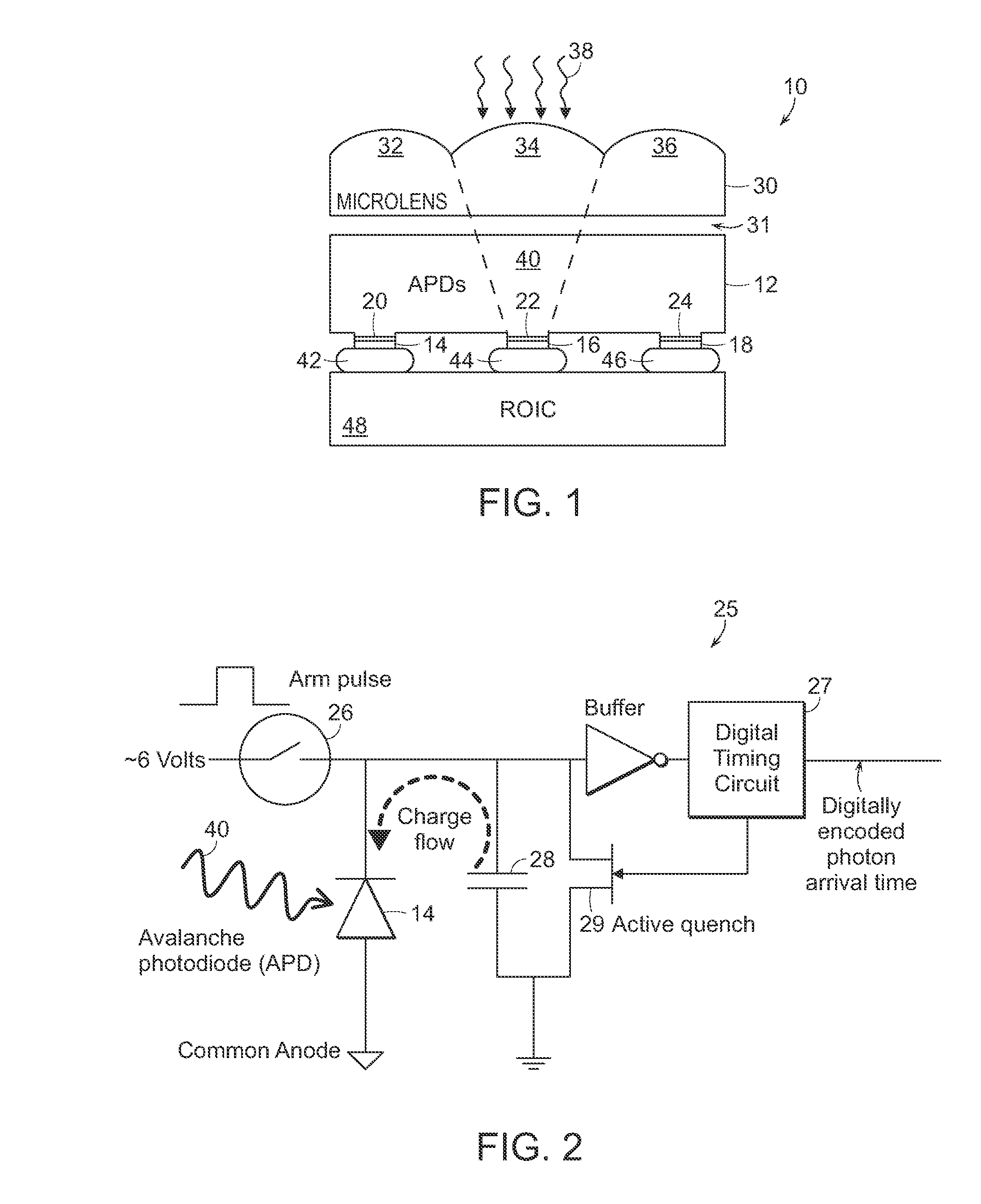
One limitation of such densely packed Geiger-mode APDs arrays is optical cross-talk.
As Geiger-mode APD array size, density, and performance requirements increase, optical cross-talk becomes an increasingly limiting source of such secondary photon detection.

Method used


Image

  • Cross-Talk Suppression in Geiger-Mode Avalanche Photodiodes
  • Cross-Talk Suppression in Geiger-Mode Avalanche Photodiodes
  • Cross-Talk Suppression in Geiger-Mode Avalanche Photodiodes

Examples


example 1

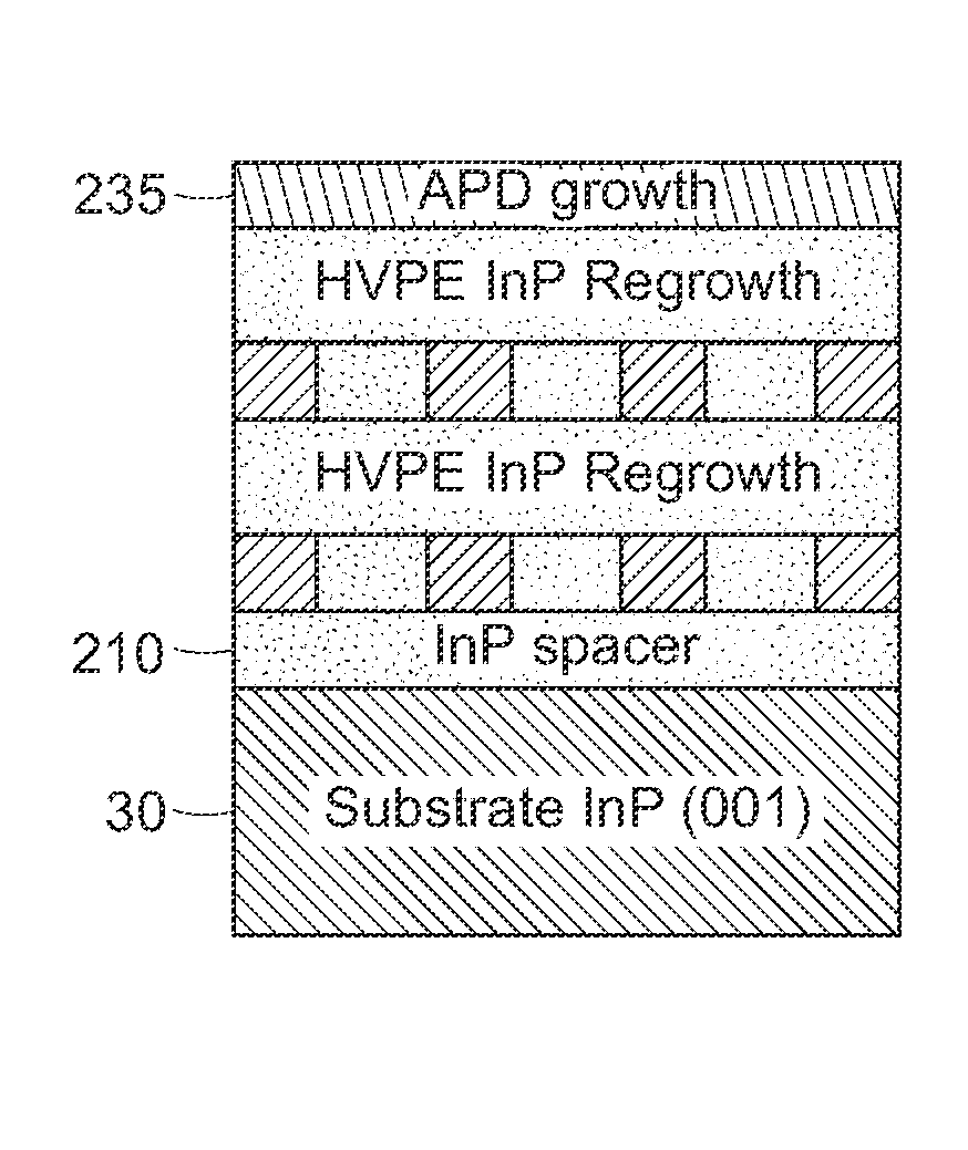
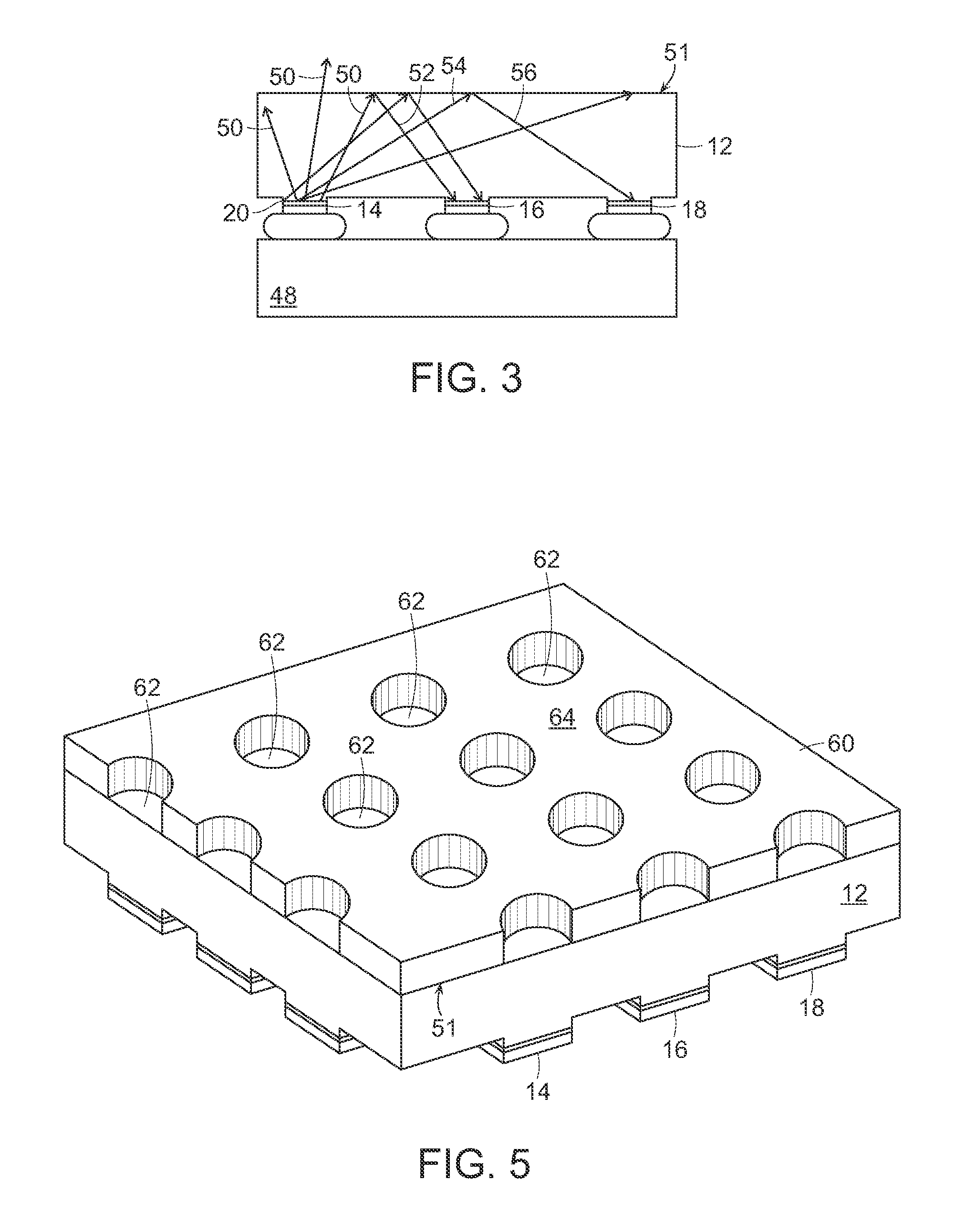
[0048]An APD array substrate of InP was fabricated with mesa photodiodes of the SAM configuration and with no back side surface cross-talk blocking layer. A second InP APD array was similarly produced but was provided with a back-surface cross-talk blocking layer having 40 micron-diameter circular openings, each opening located above an underlying photodiode mesa, with a resulting 50 micron-pitch. The back surface cross-talk blocking layer consisted of a blanket coating of titanium of 50 nm in thickness and a blanket coating of gold of 250 nm in thickness, with the circular openings produced by lift-off photolithography on the titanium and gold layers.

[0049]The optical cross-talk between neighboring photodiodes in a 9×9 area was determined for each of the APD arrays as a function of applied over bias to each photodiode for arming the photodiodes above breakdown to detect incoming photons. FIG. 7 is a plot of an integrated cross-talk probability corresponding to this determination. S...


PUM


Abstract

An avalanche photodiode detector is provided with a substrate including an array of avalanche photodiodes. An optical interface surface of the substrate is arranged for accepting external input radiation. There is provided at least one cross-talk blocking layer of material including apertures positioned to allow external input radiation to reach photodiodes and including material regions positioned for attenuating radiation in the substrate that is produced by photodiodes in the array. Alternatively at least one cross-talk blocking layer of material is disposed on the optical interface surface of the substrate to allow external input radiation to reach photodiodes and attenuate radiation in the substrate that is produced by photodiodes in the array. At least one cross-talk filter layer of material can be disposed in the substrate adjacent to the photodiode structures, including a material that absorbs radiation in the substrate that is produced by photodiodes in the array.

Description

CROSS-REFERENCE TO RELATED APPLICATIONS[0001]This application is a continuation of co-pending U.S. application Ser. No. 12 / 771,155, filed Apr. 30, 2010, which claims the benefit of U.S. Provisional Application No. 61 / 214,934, filed Apr. 30, 2009, the entirety of which is hereby incorporated by reference.STATEMENT REGARDING FEDERALLY SPONSORED RESEARCH[0002]This invention was made with Government support under Contract No. FA8721-05-C-0002 awarded by the Department of Defense. The Government has certain rights in the invention.BACKGROUND OF INVENTION[0003]This invention relates generally to electronic photodiodes, and more particularly relates to avalanche photodiodes such as Geiger-mode avalanche photodiodes.[0004]Avalanche photodiodes (APDs) operating in Geiger-mode (GM) can be employed to detect single infrared photon arrival with sub-nanosecond accuracy. As a result, Geiger-mode avalanche photodiode arrays are receiving increased interest for a number of photon-counting applicati...

Claims


Application Information

Patent Timeline
Patent Type & Authority Applications(United States)
IPC IPC(8): H01L31/107H01L31/0216H01L31/0352H01L31/0304H01L25/16H01L31/02H01L27/144H01L31/0232
CPCH01L31/107H01L27/1446H01L31/02162H01L31/0352H01L31/03046H01L25/167H01L31/02005H01L31/02327H01L2924/0002H01L2924/00
Inventor MCINTOSH, K. ALEXANDERCHAPMAN, DAVID C.DONNELLY, JOSEPH P.OAKLEY, DOUGLAS C.NAPOLEONE, ANTONIODUERR, ERIK K.VERGHESE, SIMONYOUNGER, RICHARD D.
Owner MASSACHUSETTS INST OF TECH
Learn More