Package structure and method for manufacturing the same

a technology of packaging and encapsulation, applied in the direction of semiconductor devices, semiconductor/solid-state device details, electrical devices, etc., can solve the problems of poor luminous efficiency, poor luminous efficiency, yellowing of encapsulants, etc., to improve luminous efficiency, shorten the distance between fluorescent layers, and reduce heat generation

Inactive Publication Date: 2016-07-28
LING PEICHING
View PDF0 Cites 2 Cited by
  • Summary
  • Abstract
  • Description
  • Claims
  • Application Information

AI Technical Summary

Benefits of technology

[0014]The package structure according to the present disclosure shortens the distance between the fluorescent layer and the light emitting element by allowing the fluorescent layer to combine and be in contact with the second side of the light emitting element, thereby achieving a better luminous efficiency.
[0015]Additionally, the side faces of the light emitting element are in contact with and combined with the coating body. As a result, no light will be emitted from the side faces of the light emitting element. Therefore, the heat generated is reduced, and problems such as yellowing of the encapsulant and poor luminous efficiency due to overheating of the fluorescent powder are solved. The metal structure also improves heat dissipation.

Problems solved by technology

Moreover, the fluorescent layer 13 is separated too far from the LED 11, resulting in a poor luminous efficiency.
Issues such as yellowing of the encapsulant, poor luminous efficiency due to overheating of the fluorescent powder may occur, especially for the encapsulant at a side face 11c of the LED 11.
Therefore, the heat generated is reduced, and problems such as yellowing of the encapsulant and poor luminous efficiency due to overheating of the fluorescent powder are solved.

Method used


Image

  • Package structure and method for manufacturing the same
  • Package structure and method for manufacturing the same
  • Package structure and method for manufacturing the same

Examples


Embodiment Construction

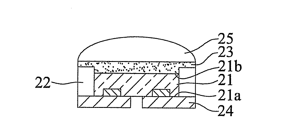
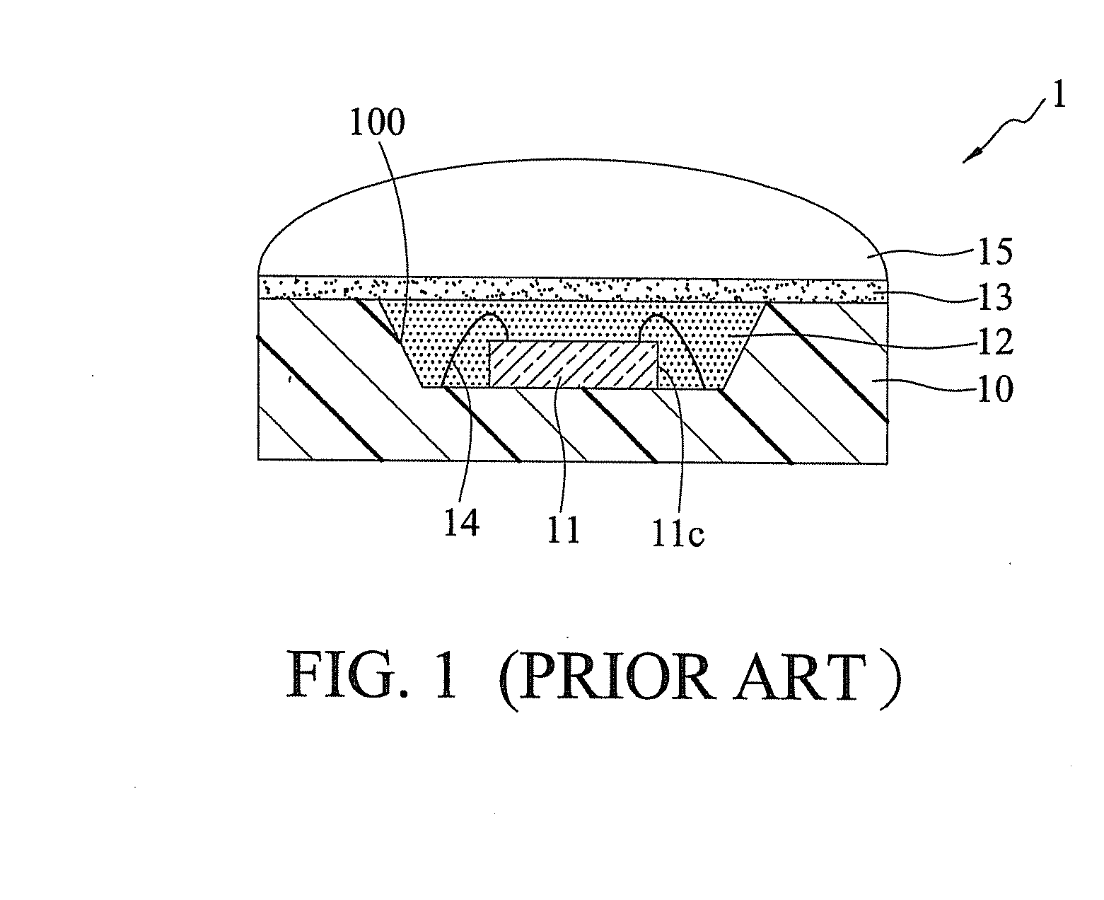
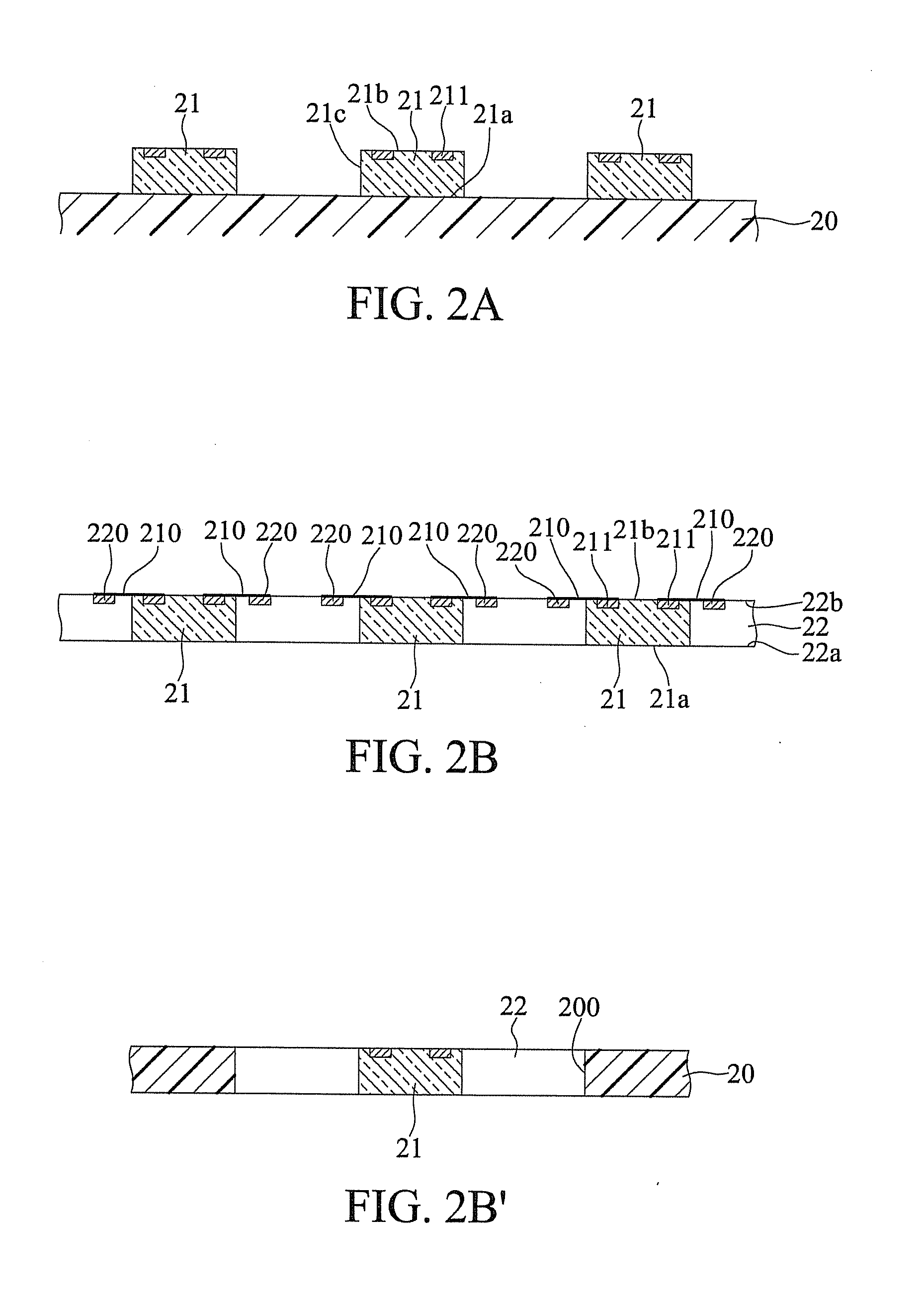
[0022]The present disclosure is described by the following specific embodiments. Those with ordinary skills in the arts can readily understand other advantages and functions of the present disclosure after reading the disclosure of this specification.

[0023]It should be noted that the structures, ratios, sizes shown in the drawings appended to this specification are to be construed in conjunction with the disclosure of this specification in order to facilitate understanding of those skilled in the art. They are not meant, in any ways, to limit the implementations of the present disclosure, and therefore have no substantial technical meaning. Without affecting the effects created and objectives achieved by the present disclosure, any modifications, changes or adjustments to the structures, ratio relationships or sizes, are to be construed as fall within the range covered by the technical contents disclosed herein. Meanwhile, terms, such as “up”, “down”, “bottom”, “first”, “second”, “a...


PUM


Abstract

A package structure is provided, which includes a light emitting element having opposite first and second sides, a coating body combined with side faces of the light emitting element, a fluorescent layer disposed on the second side, and a metal structure disposed on the first side. As the coating body is in contact with and combined with the side faces of the light emitting element, light will not be emitted from the side faces of the light emitting element. Therefore, the heat generated is reduced, and issues such as yellowing of the encapsulant and poor luminous efficiency due to overheating of the fluorescent powder are avoided. Further, the metal structure enhances the heat dissipation. A method for manufacturing the package structure is also provided.

Description

CROSS-REFERENCE TO RELATED APPLICATION[0001]The present application is based on, and claims priority from Taiwan Application Number 104102655, filed Jan. 27, 2015, the disclosure of which is hereby incorporated by reference herein in its entirety.BACKGROUND[0002]1. Technical Field[0003]The present disclosure relates to semiconductor packages, and, more particularly, to a light emitting package.[0004]2. Description of Related Art[0005]With the rapid development of the electronic industry, the form factors of the electronic products are tended towards compactness and miniaturization, while their functionalities are heading in the directions of high performance, high functionalities, and high speeds. Light Emitting Diodes (LEDs) are widely used in electronic products with lighting requirements due to advantages such as their long life, small size, high shock resistance and low power consumptions. As a result, their applications are being seen in industries, various electronic products,...

Claims


Application Information

Patent Timeline
Patent Type & Authority Applications(United States)
IPC IPC(8): H01L33/62H01L33/50H01L33/00H01L21/683H01L33/44H01L33/64H01L33/54
CPCH01L33/62H01L33/64H01L33/505H01L33/54H01L21/6835H01L33/44H01L33/0095H01L2933/0025H01L2933/0066H01L2933/0041H01L2933/005H01L2933/0075H01L33/48H01L33/50H01L33/52H01L33/647H01L33/486H01L2933/0033H01L2224/48091H01L2224/8592H01L2224/94H01L21/568H01L24/96H01L24/97H01L2224/04105H01L2224/32245H01L2224/73267H01L2224/97H01L2924/18162H01L2924/18165H01L23/3135H01L24/19H01L2924/00014H01L2224/83H01L2224/18
Inventor LING, PEICHINGLIU, DEZHONG
Owner LING PEICHING
Why Eureka
Try Eureka