
Wiring board

Inactive Publication Date: 2016-07-28
KYOCERA CORP
View PDF2 Cites 1 Cited by
  • Summary
  • Abstract
  • Description
  • Claims
  • Application Information

AI Technical Summary

Benefits of technology

The present invention aims to reduce warping of a wiring board by minimizing differences in thermal expansion and contraction behavior between conductor layers on upper and lower surfaces of a core substrate and between conductor layers formed at the same level on the upper and lower surface sides with the core substrate. This is done by making the thickness of conductor layers with a larger area occupation ratio smaller than the thickness of conductor layers with a smaller area occupation ratio between the conductor layers on the upper and lower surfaces of the core substrate and between conductor layers formed at the same level on the upper and lower surface sides with the core substrate as the center. This reduces volume differences between the conductor layers and minimizes warping of the wiring board. This results in a wiring board that can stably operate semiconductor elements and ensure a strong connection with solder.

Problems solved by technology

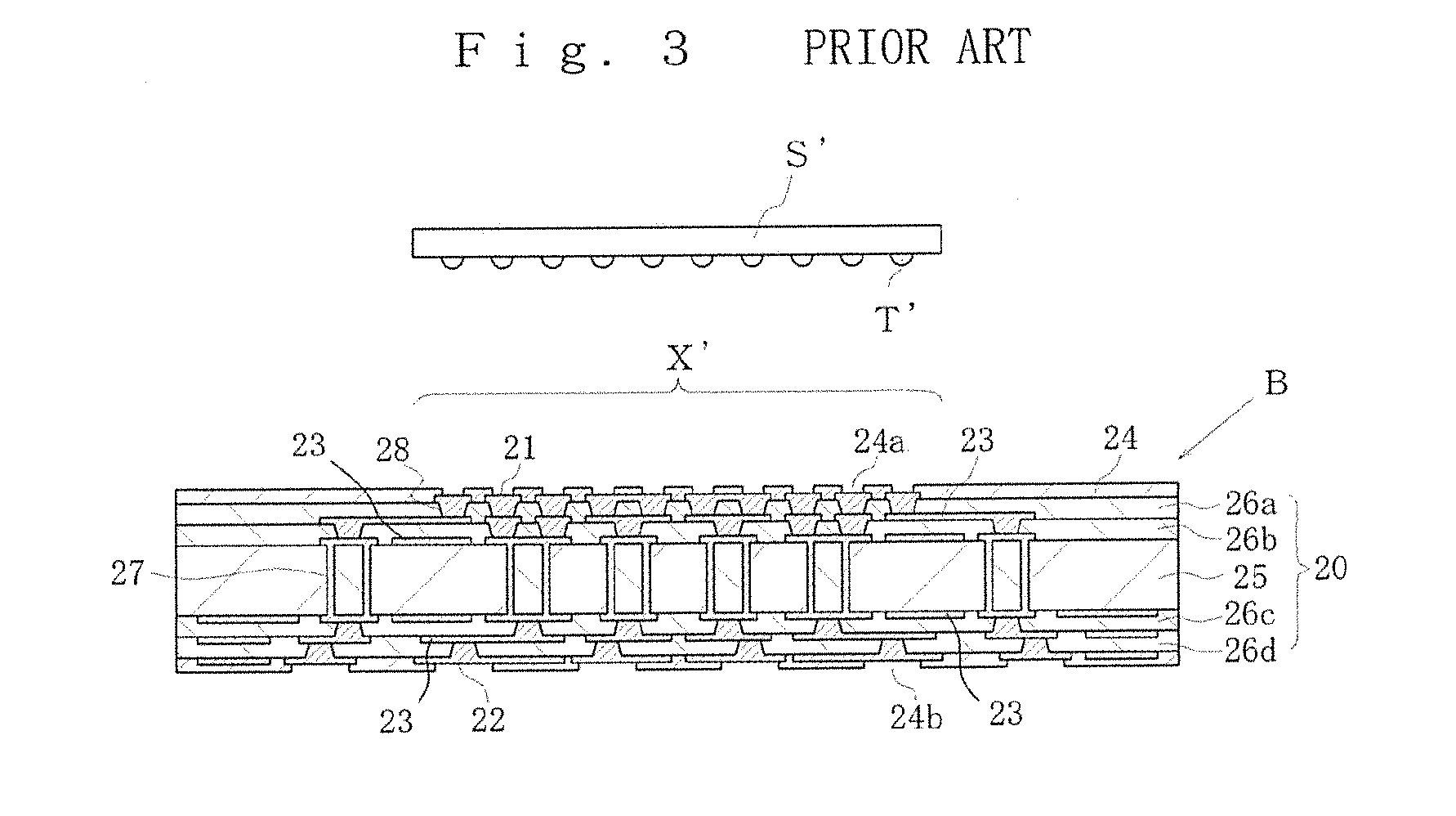
This leads to the problem that it is difficult to surely weld the solder to the electrode T′ and the semiconductor element connection pads 21, thus failing to achieve a stable operation of the semiconductor element.

Method used


Image

  • Wiring board
  • Wiring board
  • Wiring board

Examples


Embodiment Construction

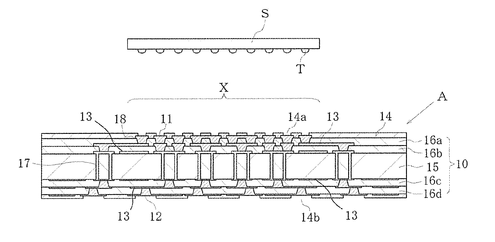
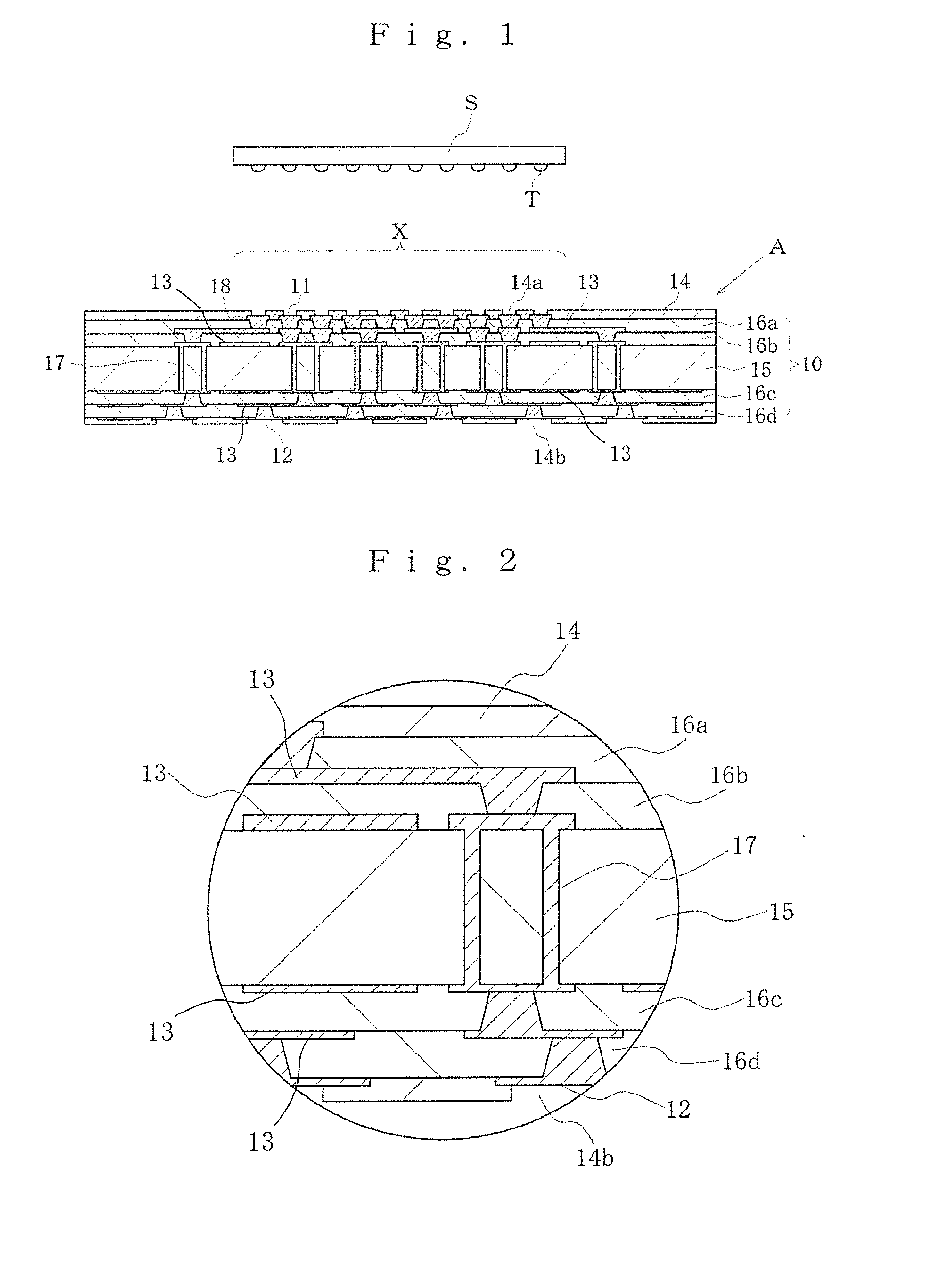
[0019]A wiring board according to the one embodiment is described with reference to FIG. 1. The wiring board A shown in FIG. 1 includes an insulating substrate 10, a conductor layer 13, and a solder resist layer 14.

[0020]The insulating substrate 10 is obtained by laminating insulating layers 16a and 16b on an upper surface of a core substrate 15, and insulating layers 16c and 16d on a lower surface of the core substrate 15. The insulating substrate 10 has a mounting portion X for mounting a semiconductor element S at a central portion on an upper surface thereof. The core substrate 15 is formed of an electrical insulating material obtained by, for example, impregnating a glass cloth with epoxy resin, bismaleimide triazine resin, or the like, followed by curing.

[0021]The core substrate 15 has a plurality of through holes 17. The conductor layer 13 is deposited on upper and lower surfaces of the core substrate 15 and in the through holes 17. The through holes 17 are formed by, for exa...


PUM


Abstract

A wiring board of the present invention includes a core substrate, insulating layers laminated on upper and lower surfaces of the core substrate, and a conductor layer deposited on the upper and lower surfaces of the core substrate and a surface of each of the insulating layers, in such a manner as to make a difference in area occupation ratio between the upper and lower surfaces of the core substrate. A thickness of a conductor that has a large area occupation ratio is smaller than a thickness of a conductor that has a small area occupation ratio between the conductor layers deposited on the upper and lower surfaces of the core substrate, and between the conductor layers deposited on the surface of each of the insulating layers laminated at an identical level on upper and lower surface sides with the core substrate as a center.

Description

BACKGROUND OF THE INVENTION[0001]1. Field of the Invention[0002]The present invention relates to a wiring board for mounting a semiconductor element.[0003]2. Description of the Related Art[0004]FIG. 3 shows a conventional wiring board B for mounting a semiconductor element S′. The wiring board B includes an insulating substrate 20, a conductor layer 23, and a solder resist layer 24.[0005]The insulating substrate 20 is obtained by laminating insulating layers 26a and 26b on an upper surface of a core substrate 25, and insulating layers 26c and 26d on a lower surface of the core substrate 25. The insulating substrate 20 has a mounting portion X′ for mounting the semiconductor element S′ at a central portion. The core substrate 25 is formed of an electrical insulating material obtained by, for example, impregnating a glass cloth with epoxy resin, bismaleimide triazine resin, or the like, followed by curing.[0006]The core substrate 25 has a plurality of through holes 27. The core substr...

Claims


Application Information

Patent Timeline
IPC IPC(8): H05K1/02
CPCH05K1/0213H05K1/09H05K2201/0338H01L2224/16225H01L2924/15174H05K1/0271H05K3/3436H05K3/4644H05K2201/09736
Inventor ITOH, YASUKI
Owner KYOCERA CORP
Learn More