Printed circuit board with embedded electronic component and manufacturing method thereof

a technology of printed circuit boards and electronic components, applied in the direction of printed capacitor incorporation, printed circuit non-printed electric components association, semiconductor/solid-state device details, etc., can solve the problem that electronic products are hindered from being truly multi-functional

Active Publication Date: 2016-07-28
SAMSUNG ELECTRO MECHANICS CO LTD
View PDF3 Cites 31 Cited by
  • Summary
  • Abstract
  • Description
  • Claims
  • Application Information

AI Technical Summary

Benefits of technology

[0008]This Summary is provided to introduce a selection of concepts in a simplified form that are further described below in the Detailed Description. This Summary is not inten

Problems solved by technology

However, as the mounting area is too small to mount multiple devices in the conventiona

Method used


Image

  • Printed circuit board with embedded electronic component and manufacturing method thereof
  • Printed circuit board with embedded electronic component and manufacturing method thereof
  • Printed circuit board with embedded electronic component and manufacturing method thereof

Examples


Embodiment Construction

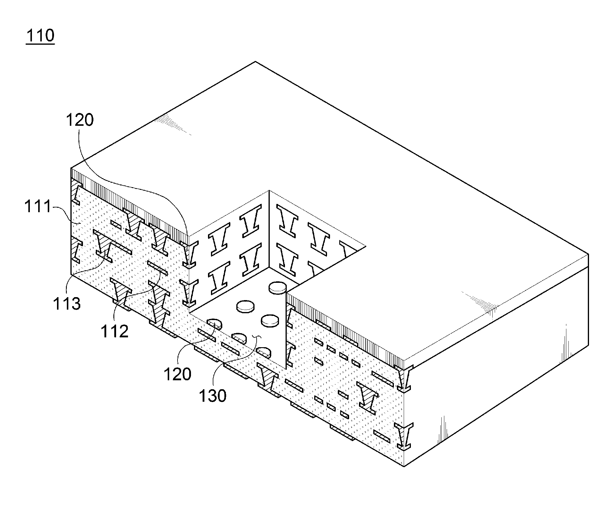
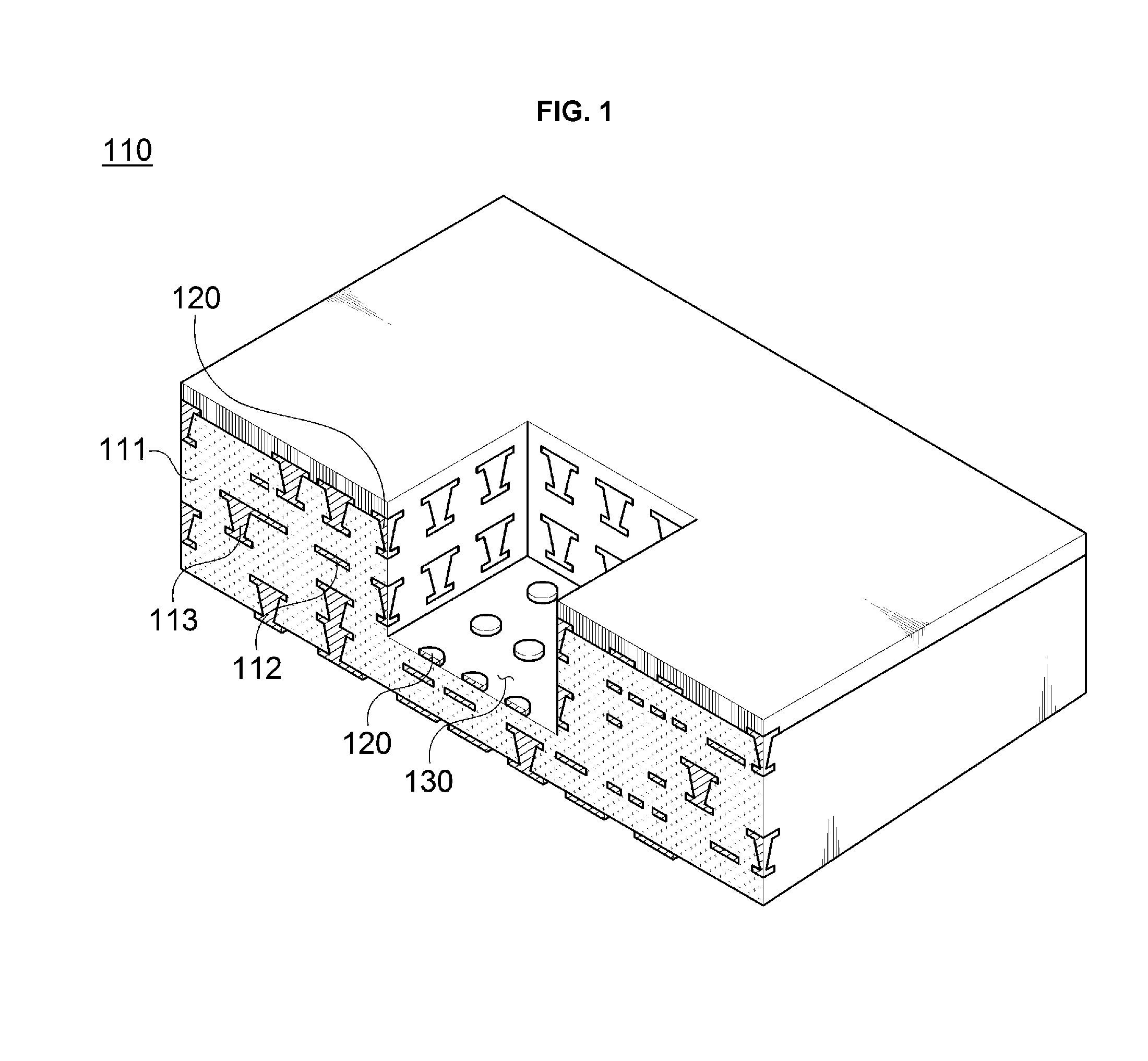
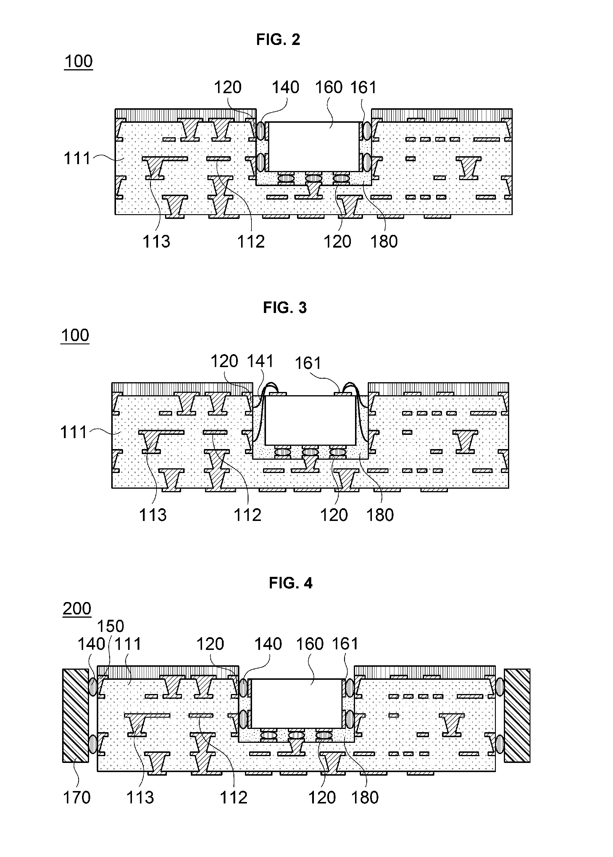
[0039]The following detailed description is provided to assist the reader in gaining a comprehensive understanding of the methods, apparatuses, and / or systems described herein. However, various changes, modifications, and equivalents of the methods, apparatuses, and / or systems described herein will be apparent to one of ordinary skill in the art. The sequences of operations described herein are merely examples, and are not limited to those set forth herein, but may be changed as will be apparent to one of ordinary skill in the art, with the exception of operations necessarily occurring in a certain order. Also, descriptions of functions and constructions that are well known to one of ordinary skill in the art may be omitted for increased clarity and conciseness.

[0040]The features described herein may be embodied in different forms, and are not to be construed as being limited to the examples described herein. Rather, the examples described herein have been provided so that this disc...


PUM


Abstract

A printed circuit board including an electronic component and a method of producing the same are provided. The printed circuit board includes a multilayered substrate including an insulation layer and an inner circuit layer laminated therein, a cavity disposed in the multilayered substrate, a via disposed in the insulation layer and configured to electrically connect the inner circuit layer with another inner circuit layer, a first electronic component inserted in the cavity, and a bump pad disposed on a surface of the cavity facing the first electronic component, and the bump pad is formed by having the insulation layer and the via exposed to a lateral side of the cavity.

Description

CROSS-REFERENCE TO RELATED APPLICATIONS[0001]This application claims the benefit under 35 USC 119(a) of Korean Patent Application No. 10-2015-0011203, filed on Jan. 23, 2015, in the Korean Intellectual Property Office, the entire disclosure of which is incorporated herein by reference for all purposes.BACKGROUND[0002]1. Field[0003]The following description relates to a printed circuit board including a multilayered board with a cavity in which an electronic component is embedded and a method of manufacturing the printed circuit board.[0004]2. Description of Related Art[0005]With the widespread use of smaller, slimmer and more integrated electronic products, the printed circuit package boards used in the electronic products have also become increasingly smaller and slimmer.[0006]To produce electronic products that are multi-functional at lower costs, multiple chips are mounted on multilayered substrates, in which a plurality of circuit layers are formed. To accommodate the chips, a g...

Claims


Application Information

Patent Timeline
IPC IPC(8): H05K1/18H05K3/46H05K3/32H05K1/11H05K3/30
CPCH05K1/183H05K1/115H05K3/4697H05K3/32H05K3/30H05K1/182H05K2201/0919H05K2201/09381H01L2224/48091H01L2224/49109H01L2224/73257H01L2924/00014H01L24/14H01L24/17H01L24/49H01L23/3121H01L2224/16227H01L2224/17183H01L2924/15153H01L2224/81815H01L2224/73204H01L2224/32105H01L2224/8114H01L2924/19101H01L24/13H01L2224/13011H01L2224/13195H01L2224/13644H01L2224/13639H01L2224/13693H01L2224/1379H01L2224/138H01L2224/81191H01L2224/81192H01L2224/14183H01L24/16H01L24/32H01L24/48H01L24/73H01L24/05H01L24/06H01L2224/06183H01L2224/0401H01L2224/81121H01L24/81H01L2924/3841H01L2224/131H01L2224/05599H01L2224/81399H01L2224/83399H01L2224/451H01L2224/2919H01L2224/45099H01L2924/00012H01L2924/01006H01L2924/0665H01L2924/014H01L2924/06H05K1/0298H05K1/185H05K3/284H05K2201/10H05K2201/1003H05K1/162H05K2201/10007H05K2201/10022H01L2224/16225H01L2224/14H01L2224/17H01L23/00
Inventor KO, KYUNG-HWANKO, YOUNG-GWANLEE, JAE-EANMOK, JEE-SOOBAEK, YONG-HO
Owner SAMSUNG ELECTRO MECHANICS CO LTD
Why Eureka
Try Eureka