Electrostatic discharge protection structure in a semiconductor device

Active Publication Date: 2016-08-04
SEMICON MFG INT (SHANGHAI) CORP
View PDF9 Cites 7 Cited by
  • Summary
  • Abstract
  • Description
  • Claims
  • Application Information

AI Technical Summary

Benefits of technology

[0015]The following description, together with the accompanying drawings, will pro

Problems solved by technology

The size of MOS devices continue to shrink.
Electrostatic discharge (ESD) poses a more and more significant harm to integrated circuits.
According to statistics, 35 percent of the product failure in integrated circuits is due to ESD problems.
However, with the continuing development o

Method used


Image

  • Electrostatic discharge protection structure in a semiconductor device
  • Electrostatic discharge protection structure in a semiconductor device
  • Electrostatic discharge protection structure in a semiconductor device

Examples


first embodiment

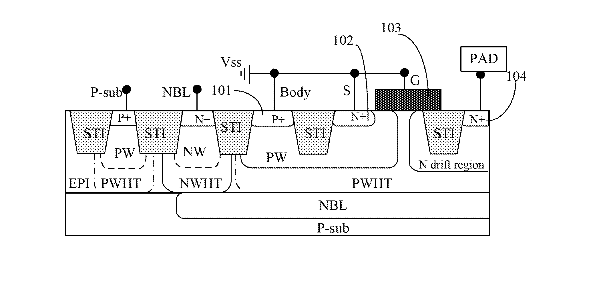
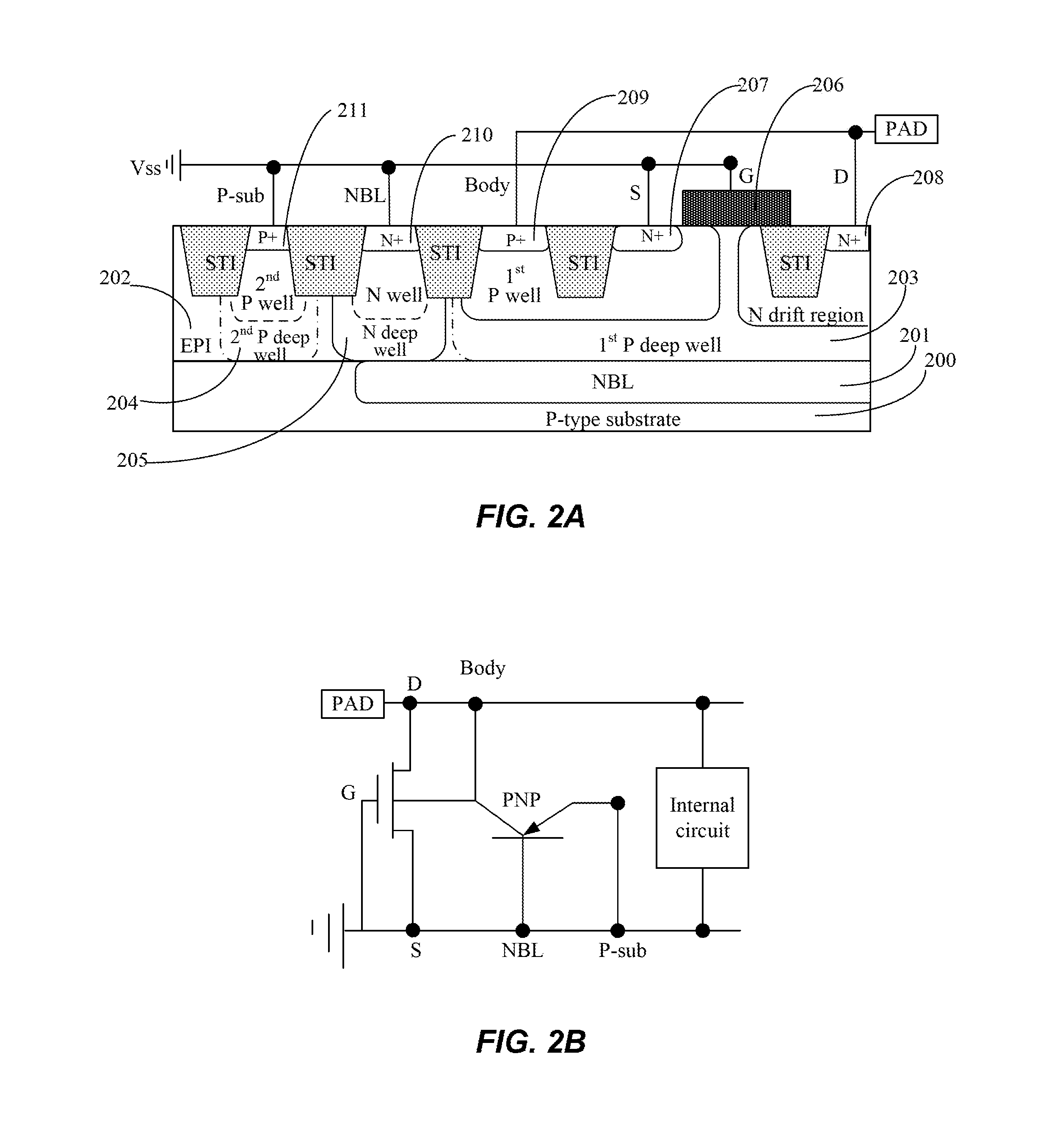
[0029]With reference to FIGS. 2A and 2B, an electrostatic discharge (ESD) protection structure according to an embodiment of the present invention will be described in detail.

[0030]The electrostatic discharge protection structure includes an LDMOS device. The LDMOS device includes an embedded bipolar junction transistors (BJT). The gate, the source, the buried layer lead-out area, and the substrate lead-out area of the LDMOS device are grounded. The drain and the body region lead-out area of the LDMOS are electrically connected to the pad input / output terminal (shown as “PAD” in FIG. 2A). In an embodiment, the bipolar junction transistor is a PNP transistor.

[0031]With reference to FIG. 2A, the LDMOS device is an NLDMOS, according to an embodiment.

[0032]The NLDMOS device includes a P-type substrate 200, an N-type buried layer (NBL) 201 formed in the P-type substrate 200, and an epitaxial (EPI) layer 202 formed above the N-type buried layer 201. The NLDMOS device further includes an N...

second embodiment

[0038]According to another embodiment of the present invention, an electronic apparatus is provided. The electronic apparatus includes the electrostatic discharge protection structure described above, and an electronic component assembly coupled to the electrostatic discharge protection structure.

[0039]The electrostatic discharge protection structure includes an LDMOS device. The LDMOS device includes an embedded bipolar junction transistors. The gate, the source, the buried layer lead-out area, and the substrate lead-out area of the LDMOS device are grounded. The drain and the body region lead-out area of the LDMOS device are electrically connected to the pad input / output terminal. According to an embodiment, the bipolar junction transistor is a PNP transistor. The LDMOS device is an NLDMOS device.

[0040]Since the electrostatic discharge protection structure provides better ESD protection, the electronic apparatus also has the advantages described above.

[0041]The electronic apparatu...


PUM


Abstract

An electrostatic discharge protection structure includes a laterally diffused metal oxide semiconductor (LDMOS) device. The LDMOS device includes an embedded bipolar junction transistor. A gate, a source, a buried layer lead-out area, and a substrate lead-out area of the LDMOS device are grounded. A drain and a body region lead-out area of the LDMOS device are electrically connected to a pad input/output terminal. In an embodiment, the embedded bipolar junction transistor includes a PNP transistor operative to transmit a reverse electrostatic discharge current. An N+ drain, a gate, an N+ source, and a P+ substrate lead-out area form a grounded-gate NMOS (GGNMOS) operative to transmit a forward electrostatic discharge current.

Description

CROSS-REFERENCES TO RELATED APPLICATIONS[0001]This application claims priority to Chinese patent application No. 201510053595.1, filed on Feb. 2, 2015, the content of which is incorporated herein by reference in its entirety.BACKGROUND OF THE INVENTION[0002]The present invention relates to semiconductor technologies, more particularly to an electrostatic discharge protection structure in a semiconductor device.[0003]In the integrated circuit chip manufacturing and the final application systems, with the continuing improvement of the VLSI technology, the current complementary metal oxide semiconductor (CMOS) integrated circuit design has entered the ultra-deep submicron stage. The size of MOS devices continue to shrink. Electrostatic discharge (ESD) poses a more and more significant harm to integrated circuits. According to statistics, 35 percent of the product failure in integrated circuits is due to ESD problems. Thus, ESD protection becomes especially important in integrated circu...

Claims


Application Information

Patent Timeline
IPC IPC(8): H01L27/02H01L27/06H01L29/78
CPCH01L27/0266H01L27/0623H01L29/7816H01L27/0259H01L27/027H01L29/7835
Inventor GAN, ZHENGHAO
Owner SEMICON MFG INT (SHANGHAI) CORP
Why Eureka
Try Eureka