
Semiconductor structure having a center dummy region

a technology of dummy region and semiconductor, which is applied in the direction of semiconductor devices, semiconductor/solid-state device details, electrical apparatus, etc., can solve the problem that current planar fets no longer meet the requirements of products

Active Publication Date: 2016-08-18
UNITED MICROELECTRONICS CORP
View PDF0 Cites 4 Cited by
  • Summary
  • Abstract
  • Description
  • Claims
  • Application Information

AI Technical Summary

Benefits of technology

The semiconductor structure with dummy slot contacts enables precise placement of slot contacts between functional regions, enhancing electrical performance by avoiding short or bridging problems, thereby improving the manufacturing process and device reliability.

Problems solved by technology

However, with the increasing miniaturization of electronic products, current planar FETs no longer meet the requirements of the products.

Method used


Image

  • Semiconductor structure having a center dummy region
  • Semiconductor structure having a center dummy region
  • Semiconductor structure having a center dummy region

Examples


Embodiment Construction

[0016]To provide a better understanding of the presented invention, preferred embodiments will be made in detail. The preferred embodiments of the present invention are illustrated in the accompanying drawings with numbered elements.

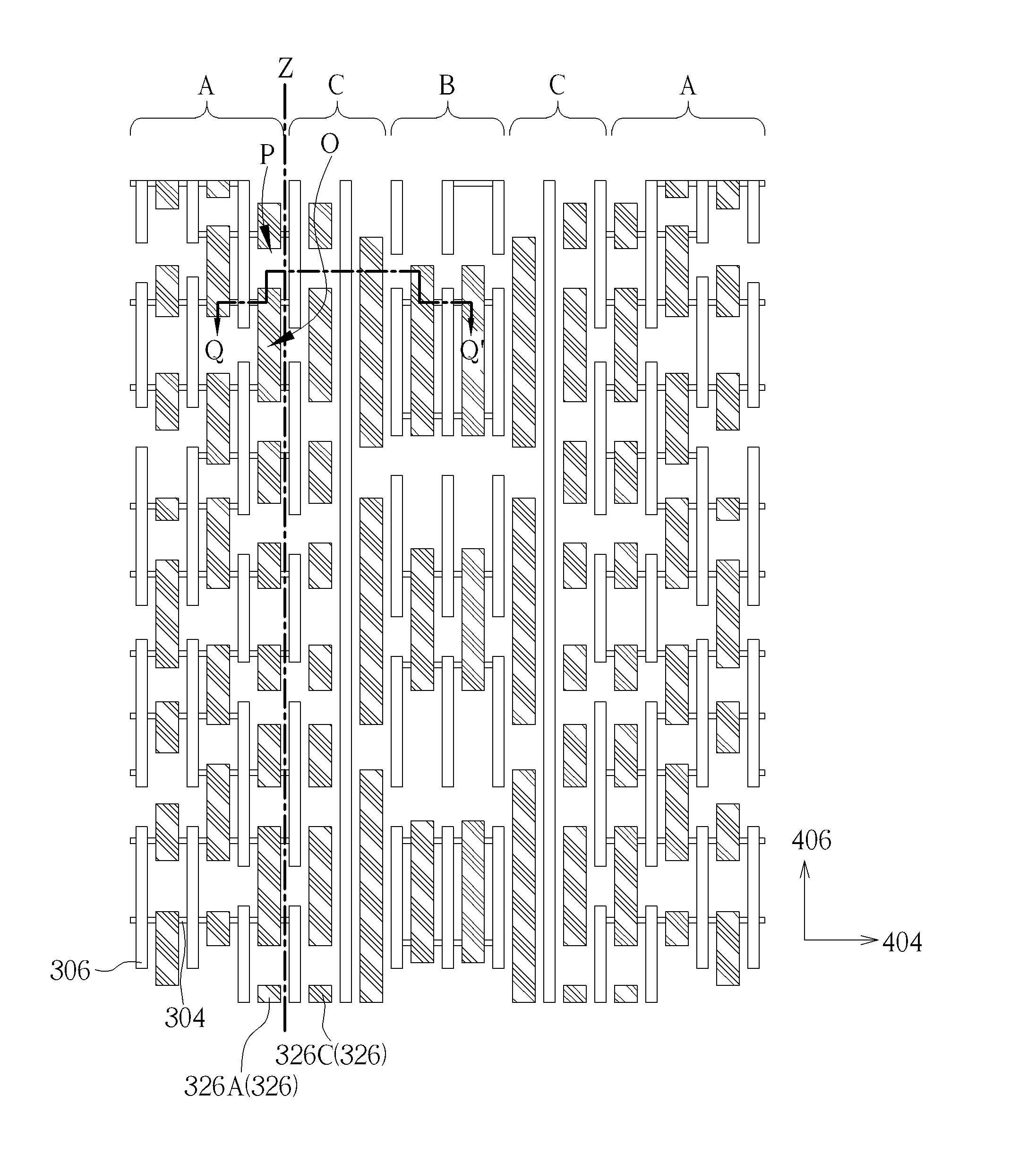
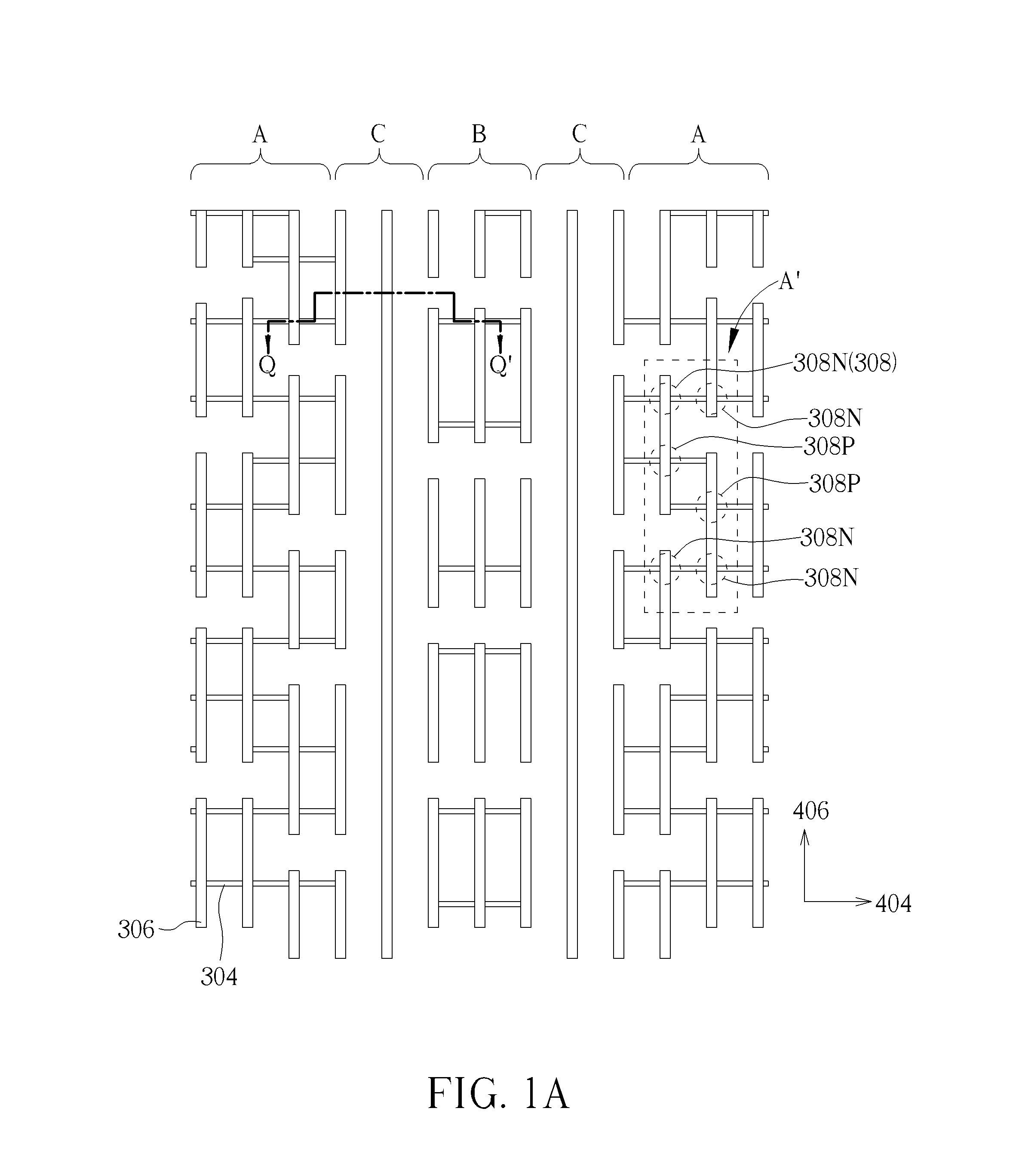
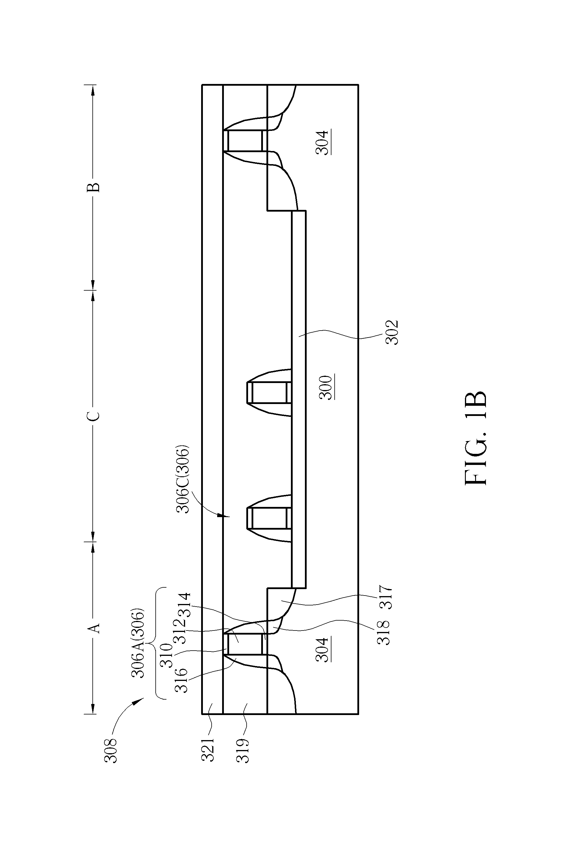
[0017]Please see FIG. 1A, FIG. 1B, FIG. 2A, FIG. 2B, FIG. 3A, FIG. 3B, FIG. 4A and FIG. 4B showing schematic diagrams of the semiconductor structure and method for forming the same according to the first embodiment of the present invention, wherein FIG. 1A, FIG. 2A, FIG. 3A, FIG. 4A are top view, and FIG. 1B, FIG. 2B, FIG. 3B, FIG. 4B are cross-sectional view taken along line QQ′ of FIG. 1A, FIG. 2A, FIG. 3A, FIG. 4A, FIG. 5A, respectively.

[0018]Please see FIG. 1A and FIG. 1B first. A substrate 300 is provided to serve as a base for forming devices, components, or circuits. The substrate 300 is preferably composed of a silicon containing material. Silicon containing materials include, but are not limited to, Si, single crystal Si, polycrystalline Si, SiG...


PUM


Abstract

A semiconductor structure is provided, including a substrate, a plurality of first semiconductor devices, a plurality of second semiconductor devices, and a plurality of dummy slot contacts. The substrate has a device region, wherein the device region includes a first functional region and a second functional region, and a dummy region is disposed therebetween. The first semiconductor devices and a plurality of first slot contacts are disposed in the first functional region. The second semiconductor devices and a plurality of second slot contacts are disposed in the second functional region. The dummy slot contacts are disposed in the dummy region.

Description

BACKGROUND OF THE INVENTION[0001]1. Field of the Invention[0002]The present invention is related to a semiconductor structure, and more particularly, to a semiconductor structure having dummy slot contacts in dummy regions.[0003]2. Description of the Prior Art[0004]In recent years, as various kinds of consumer electronic products are being constantly modified towards increased miniaturization, the size of semiconductor components are modified to be reduced accordingly, in order to meet high integration, high performance, low power consumption, and the demands of products.[0005]However, with the increasing miniaturization of electronic products, current planar FETs no longer meet the requirements of the products. Thus, non-planar FETs such as Fin-shaped FETs (Fin-FET) have been developed, which includes a three-dimensional channel structure. The manufacturing processes of Fin-FET devices can be integrated into traditional logic device processes, and thus are more compatible. In addit...

Claims


Application Information

Patent Timeline
Patent Type & Authority Applications(United States)
IPC IPC(8): H01L27/11H01L29/06H01L23/535H01L29/78H10B10/00
CPCH01L27/1104H01L29/7851H01L29/66545H01L23/535H01L27/3223H01L29/0649H01L21/823821H01L21/845H01L27/0924H01L27/1211H10K59/88H10B10/12
Inventor HUNG, CHING-WENWU, JIA-RONGLEE, YI-HUIHUANG, CHIH-SENCHEN, YI-WEI
Owner UNITED MICROELECTRONICS CORP
Learn More