Memory device and storage apparatus

a memory device and storage device technology, applied in the field of memory devices and storage devices, can solve the problems of high cost of ssd, high number of upper limit, and inability to meet the needs of large-scale storage, etc., and achieve the effect of increasing capacity, high quality, and large available capacity

Active Publication Date: 2016-09-08
HITACHI LTD
View PDF3 Cites 15 Cited by
  • Summary
  • Abstract
  • Description
  • Claims
  • Application Information

AI Technical Summary

Benefits of technology

[0006]With the technology of PTL 1, when a failure occurs in a part of a non-volatile semiconductor memory in a memory device, the memory device is closed even in the presence of a large number of other available parts (a die or a chip of the memory), each having high quality. This results in a need for such a memory device to be replaced. As a capacity is increased in a memory device, an available capacity still remains to be large even when a failure occurs in a partial area. Therefore, the closing of the memory device for the partial failure results in a lot of wasting. With the occurrence of the failure, accordingly, there is a possibility of avoiding the closure of the memory device provided that a controller in the memory device inspects the whole non-volatile semiconductor memory to specify a failure region. However process for inspecting the whole non-volatile semiconductor memory causes a load to increase, resulting in performance degradation of the memory device.
[0007]To solve the above problem, a memory device according to an aspect of the present invention includes a plurality of non-volatile semiconductor memories, and a device controller that is coupled to the plurality of non-volatile semiconductor memories and coupled to a host apparatus which issues an instruction for accessing the plurality of non-volatile semiconductor memories. Each of the plurality of non-volatile semiconductor memories includes a plurality of storage circuits and a plurality of control circuits, the plurality of storage circuits are coupled to the device controller via the plurality of control circuits, respectively, each of the plurality of storage circuits includes a plurality of blocks, each block is a unit of erasure of data, each of the plurality of blocks includes a plurality of pages, each page is a unit of read and write of data, and the device controller is configured to, when the device controller reads data stored in a specific page in the plurality of non-volatile semiconductor memories to detect an uncorrectable error (UE) of the data stored in the specific page, execute a diagnosis process including specifying a specific storage circuit that is a storage circuit including the specific page, reading data stored in a block in a part of the specific storage circuit, and specifying, on the basis of a result of reading the data stored in the block in the part, a failure region in the specific storage circuit.

Problems solved by technology

Although the SSD is more expensive than the HDD, the SSD performs I / O process at an extremely high speed.
There is an upper limit on the number of times that the block is erased, and when the number of times of erasure increases, it may be difficult to write data into the flash memory or it is likely that an error occurrence rate of data written into the flash memory increases.
As refinement of a flash memory chip is developed, the flash memory chip comes to possess a large capacity, and on the other hand, reliability is decreased and there occurs an issue that die-by-die or chip-by-chip quality is not consistent, for example.
The die of poor quality tends to increase an error occurrence rate and becomes unusable due to a failure even when the number of times of erasure is less than a predetermined number.
When such a failure occurs in a plurality of dies, it is not possible to ensure a storage area which stores user data and there is no choice but to close the memory device.
Thus, when an SSD becomes unusable at an earlier stage than a predetermined period, a replacement frequency may increase and a cost for purchase and maintenance of an SSD may occur.

Method used


Image

  • Memory device and storage apparatus
  • Memory device and storage apparatus
  • Memory device and storage apparatus

Examples


first embodiment

[0043]A configuration of a computer system of the present embodiment will be described, below.

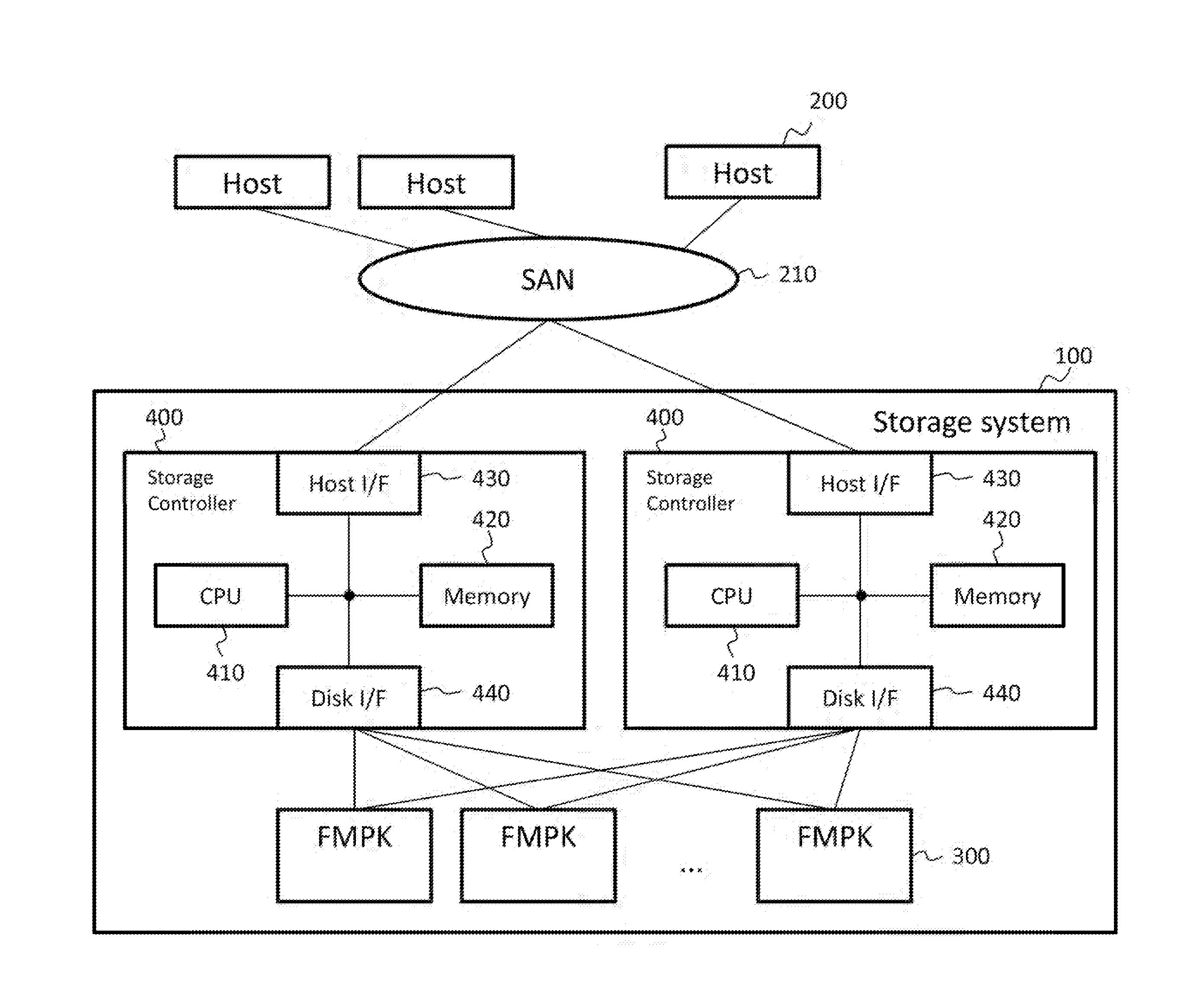
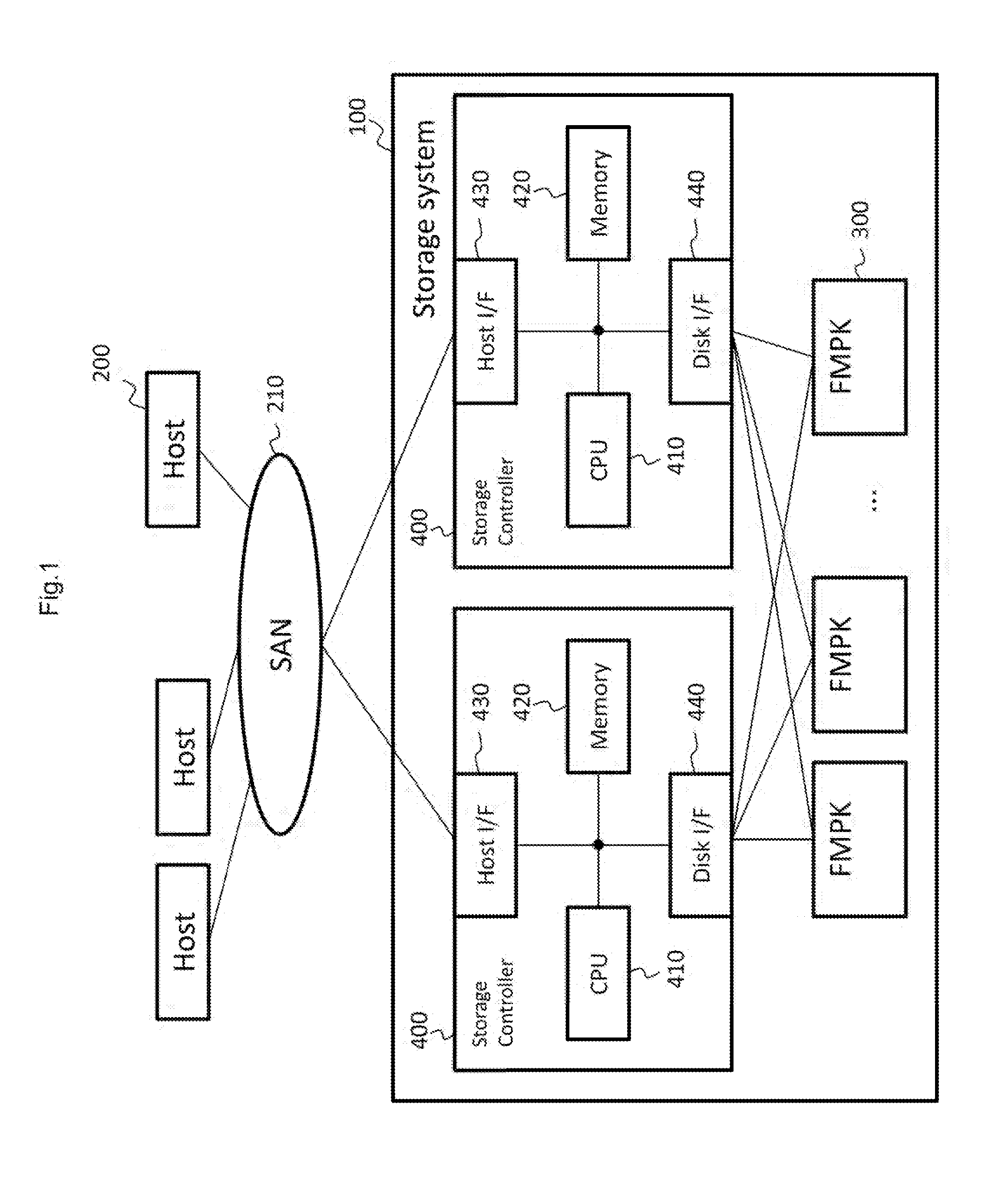
[0044]FIG. 1 shows the configuration of the computer system according to the embodiment of the present invention.

[0045]The computer system has a storage system (storage apparatus) 100, and a plurality of host computers 200. Each of the plurality of host computers 200 is coupled to the storage system 100 via a SAN (Storage Area Network) 210. The computer system may have one or more host computers 200.

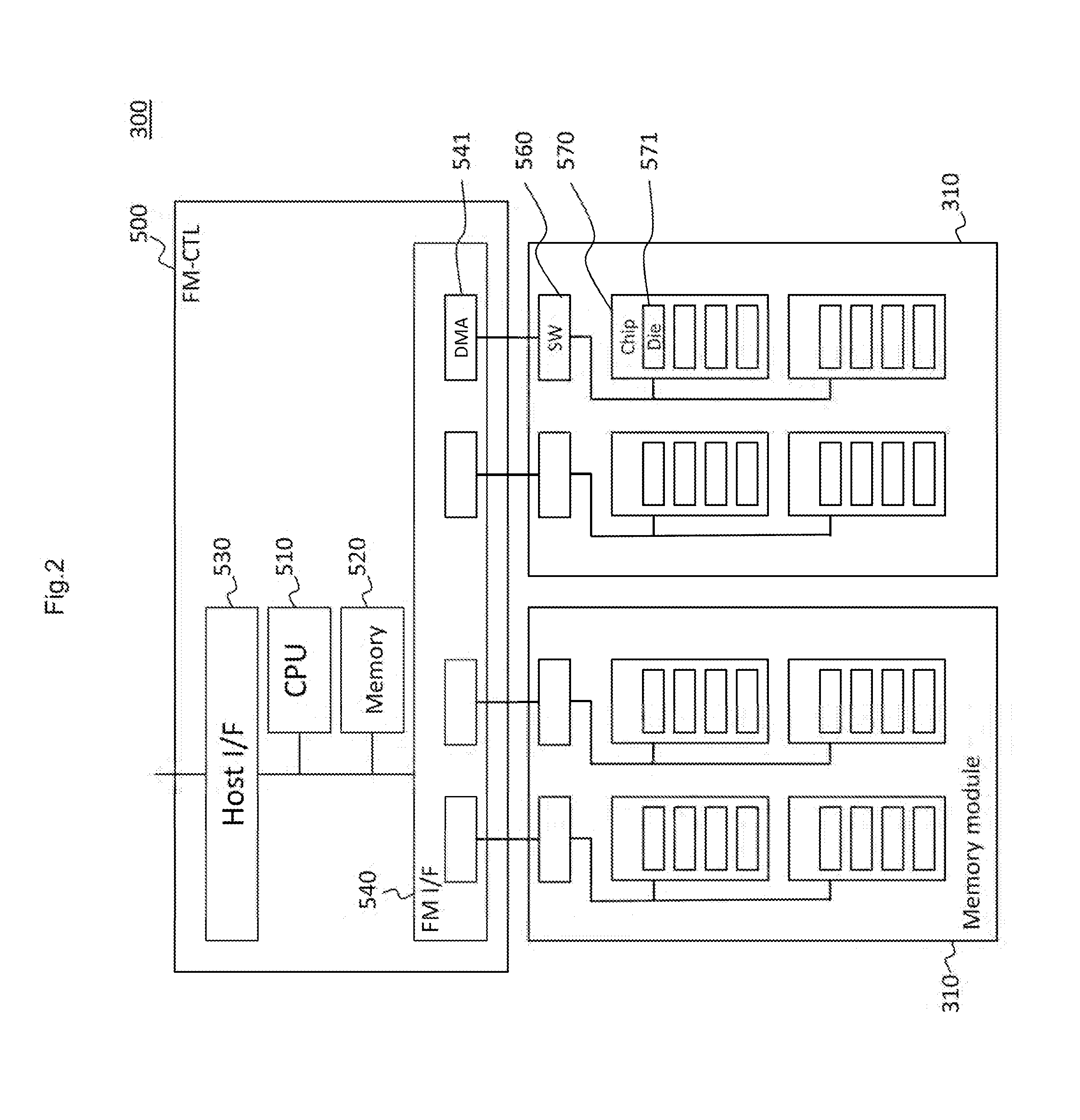
[0046]The storage system 100 has two storage controllers (DKC: Disk Controllers) 400, and a plurality of FMPKs (Flash Memory Packages) 300. The storage controller 400 is a controller which controls the plurality of memory devices, as a RAII) (Redundant Arrays of Inexpensive Disks) group (RG), for example. The two storage controllers 400 are made redundant so that one storage controller 400 controls the storage system 100 during a normal operation and the other storage controller 400 continues th...

second embodiment

[0133]The storage system 100 of the present embodiment has a similar configuration to that of the storage system 100 of the first embodiment. Description proceeds mainly with a difference from the first embodiment, below. The storage system 100 of the present embodiment changes a capacity of the FMPK 300 in response to the occurrence of a failure in the FMPK 300.

[0134]In the flash memory, the greater the capacity of the update area, the smaller the frequency of reclamation, such that the performance is maintained. However, as the capacity of the update area is large, the capacity of an area (user area) where user data is stored is decreased. That is, depending on a ratio between the capacity of the user area and the capacity of the update area, a relationship is determined between a capacity of data to be stored in the FMPK 300 by the storage controller 400, and a performance. In the description and the drawings that follow, a capacity of the user area may be referred to as a “user ...


PUM


Abstract

A failure region is specified when a failure occurs in a non-volatile semiconductor memory. When a device controller reads data stored in a specific page in a plurality of non-volatile semiconductor memories to detect an uncorrectable error (UE) of the data stored in the specific page, the device controller executes a diagnosis process including specifying a specific storage circuit that is a storage circuit including the specific page, reading data stored in a part of blocks of the specific storage circuit, and specifying, on the basis of a result of reading data stored in the block, a failure region in the specific storage circuit.

Description

TECHNICAL FIELD[0001]The present invention relates to a memory device and a storage apparatus.BACKGROUND ART[0002]In recent years, as there is an increasing amount of data to be processed in a company, a storage apparatus comes to include a large number of memory devices, and the memory device increases in capacity year by year. In general, an HDD (Hard Disk Drive) is installed as a memory device; however, in place of the HDD, in recent years, attention is focused on a memory device (an SSD: Solid State Device, for example) having, as a memory medium, a non-volatile semiconductor memory (a flash memory, for example). Although the SSD is more expensive than the HDD, the SSD performs I / O process at an extremely high speed.[0003]In the flash memory, a physical storage area is managed by a unit referred to as a “block”, and the data is erased by such block. There is an upper limit on the number of times that the block is erased, and when the number of times of erasure increases, it may ...

Claims


Application Information

Patent Timeline
Patent Type & Authority Applications(United States)
IPC IPC(8): G06F11/07
CPCG06F11/079G06F11/0751G06F11/0727G11C11/5678G11C11/5685G11C29/52G11C29/76G11C29/765
Inventor NINOSE, KENTAITOU, TAKUJIYOSHIOKA, FUMIOTSUNEHIRO, TAKASHIUEHARA, GOHOMMA, SHIGEO
Owner HITACHI LTD
Why Eureka
Try Eureka