
Active Matrix Organic Light-Emitting Diode Panel and Method for Producing CROSS

a technology of organic light-emitting diodes and active matrix, which is applied in the field of display, can solve the problems of complicated technique and scratch risk, and achieve the effect of simplifying technical procedures and avoiding scratch risk

Inactive Publication Date: 2016-09-15
EVERDISPLAY OPTRONICS (SHANGHAI) CO LTD
View PDF10 Cites 3 Cited by
  • Summary
  • Abstract
  • Description
  • Claims
  • Application Information

AI Technical Summary

Benefits of technology

The patent aims to simplify the process of mounting an integrated circuit on an AMOLED panel and to prevent scratches on the touch control cover. This is achieved by ensuring that the encapsulant layer contacts the touch control cover, and the integrated circuit is mounted on the array substrate and connected to the touch control cover. This simplifies the technical procedures required and reduces the risk of scratches on the touch control cover during the packaging process. Additionally, the transmission line and the array substrate are on the same side to avoid impact on the laser sealing process.

Problems solved by technology

Furthermore, due to the feature of self-illumination, AMOLED panels do not require backlight plates and are, thus, thinner and lighter than conventional liquid crystal panels while saving the costs for backlight modules.
Firstly, the touch control transducer serving as the medium for transmitting the touch control signals contacts the processing equipment during the packaging process, resulting in the risk of scratch.
Secondly, the junction area between the touch control transducer and the integrated circuit requires a special design to avoid influence in the laser sealing process.
Thirdly, the panels require respective integrated circuits in the cover and the substrate, which is a complicated technique.

Method used


Image

  • Active Matrix Organic Light-Emitting Diode Panel and Method for Producing CROSS
  • Active Matrix Organic Light-Emitting Diode Panel and Method for Producing CROSS
  • Active Matrix Organic Light-Emitting Diode Panel and Method for Producing CROSS

Examples


Embodiment Construction

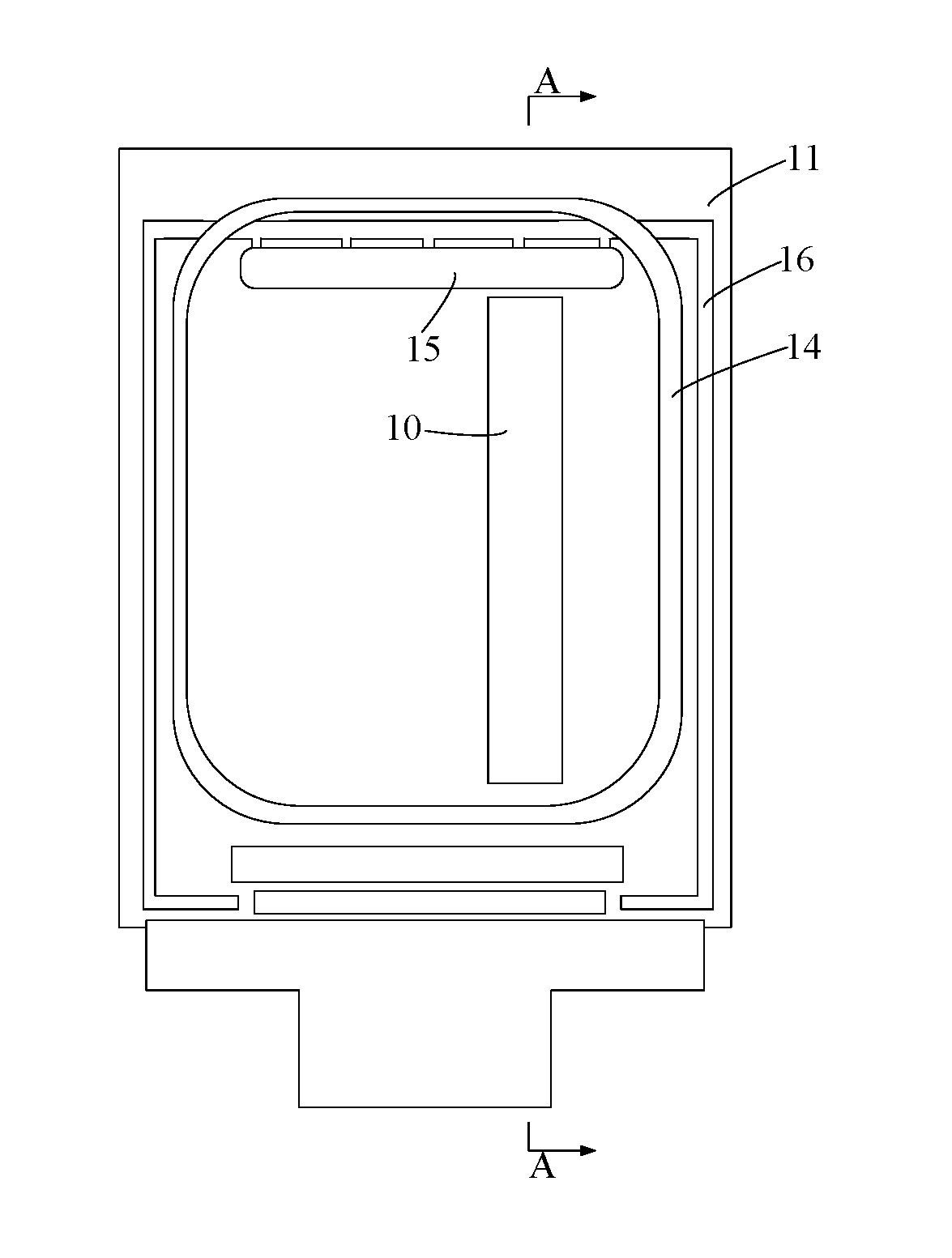
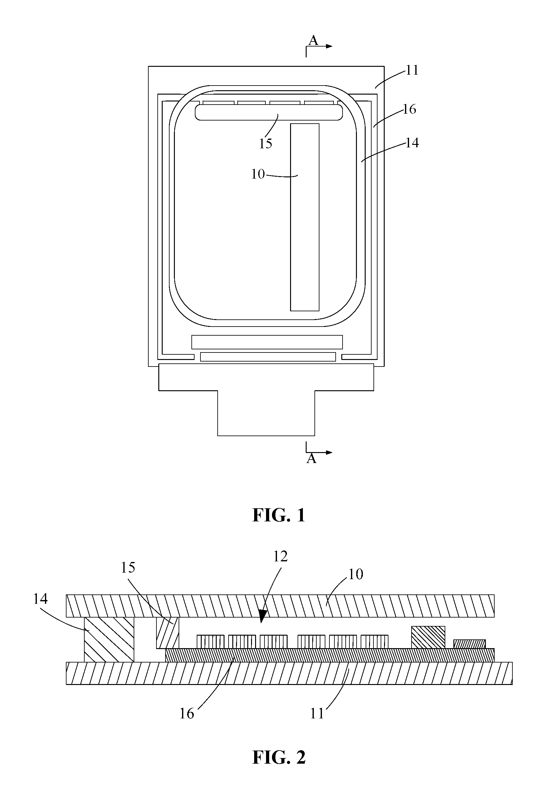
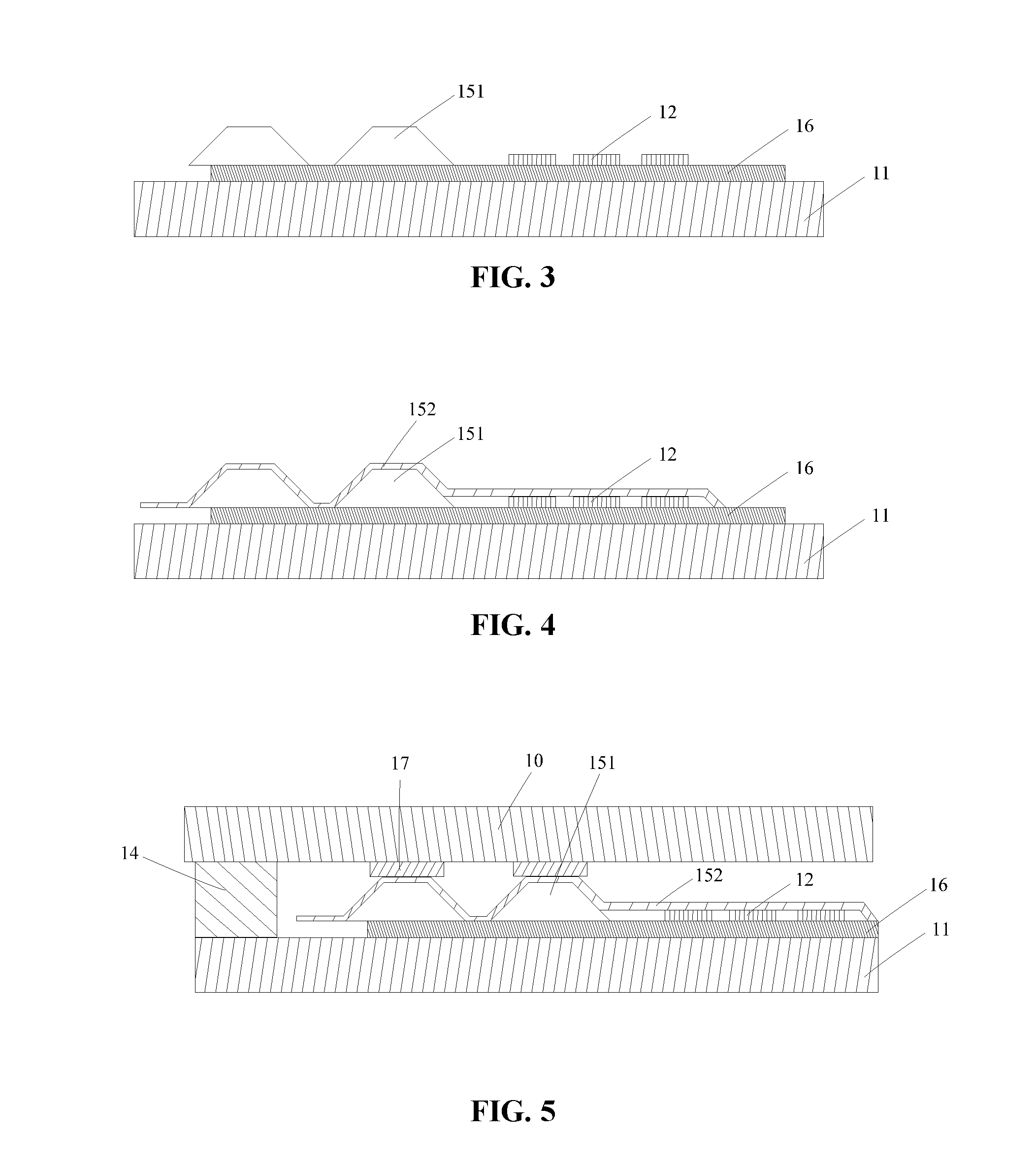
[0060]FIG. 1 is a diagrammatic view of an active matrix organic light-emitting diode (AMOLED) panel of an embodiment according to the present disclosure. The AMOLED panel according to the present disclosure includes a touch control cover 10, an AMOLED substrate, and an encapsulant layer 14. The touch control cover 10 is sealingly connected with the AMOLED substrate by the encapsulant layer 14. The touch control cover 10 with a detecting function contacting the encapsulant layer 14, such that the touch control cover 10 and the encapsulant layer 14 are on the same side during the packaging process, avoiding the risk of scratch. A lighting unit 12 and an integrated circuit controlling the lighting unit 12 are mounted on the AMOLED substrate. By electrically connecting the touch control cover to the integrated circuit, the touch control signal is sent to the integrated circuit, and the integrated circuit controls the lighting unit 12 to display. The AMOLED panel according to the present...


PUM


Abstract

An AMOLED panel and a method for producing the AMOLED panel. The AMOLED panel includes a touch control cover with a detecting function. An AMOLED substrate includes array substrate, a lighting unit mounted on the array substrate, and an integrated circuit connected to and controlling the lighting unit. The touch control cover is electrically connected to the integrated circuits. An encapsulant layer is mounted between the touch control cover and the AMOLED substrate to sealingly connect the touch control cover with the AMOLED substrate. Since the encapsulant layer contacts the touch control cover, the touch control cover and the encapsulant layer are on the same side during the packaging process, avoiding the risk of scratch. The integrated circuit mounted on the array substrate is electrically connected to the touch control cover, such that the disposition of the integrated circuit on the AMOLED panel proceeds only once.

Description

REFERENCE TO RELATED APPLICATIONS[0001]This application is based upon and claims priority to Chinese Patent Application No. 201510109875X, filed on Mar. 13, 2015, the entire contents of which are incorporated herein by reference.BACKGROUND OF THE INVENTION[0002]The present disclosure relates to the display field and, more particularly, to an active matrix organic light-emitting diode (AMOLED) panel and a method for producing the AMOLED panel.[0003]Organic light-emitting diodes (also known as organic electroluminescence) include the features of self-illumination and use a very thin coating of organic material and a very thin glass substrate. The organic material emits light when electric current passes through. In comparison with conventional liquid crystal panels, active matrix organic light-emitting diode (AMOELD) panels include the features of high speed response, high contrast, and broad view. Furthermore, due to the feature of self-illumination, AMOLED panels do not require back...

Claims


Application Information

Patent Timeline
Patent Type & Authority Applications(United States)
IPC IPC(8): H01L27/32H01L25/00H01L51/52H01L51/56G06F3/041H01L25/16
CPCH01L27/323G06F3/0412H01L27/3276H01L25/167H01L2227/323H01L51/56H01L25/50G06F2203/04103H01L51/5246H10K59/40H10K50/8426H10K50/841
Inventor ZHAO, XIAOHUZHAI, HONGFENGLIN, MAOCHUNGWANG, YENLONG
Owner EVERDISPLAY OPTRONICS (SHANGHAI) CO LTD
Learn More