ESD Protection System, Apparatus, and Method with Adjustable Trigger Voltage Decoupled from DC Breakdown Voltage

a technology of esd protection and trigger voltage, which is applied in the field of esd protection systems, methods and apparatus for improving the performance of electrostatic discharge (esd) devices, can solve the problems of limiting the use of protection devices in certain systems, and the effectiveness of such esd protection devices can be further limited by their inherent direct current breakdown voltage (dcbv), thermal meltdown/destruction of the device,

Active Publication Date: 2016-09-15
PSEMI CORP
View PDF0 Cites 10 Cited by
  • Summary
  • Abstract
  • Description
  • Claims
  • Application Information

AI Technical Summary

Benefits of technology

[0003]According to a first aspect of the present disclosure, an electrostatic discharge (ESD) protection device comprising a multiple fingers field-effect transistor (FET) is presented, the ESD protection device being configured to exhibit, during operation, a trigger voltage and a direct current breakdown voltage, wherein a finger of the multiple fingers FET comprises: a drain implantation region and corresponding drain contacts; a source implantation region and corresponding source contacts; a gate polysilicon region of length LG; and a plurality of transverse polysilicon stripes formed atop the drain implantation region and connected to the gate polysilicon region, and wherein: the gate length LG is chosen such that, during operation of the ESD protection device under an ESD event, a Zener breakdown mode of operation of the ESD protection device is provided, and a spacing between two consecutive transverse polysilicon stripes is configured to control the trigger voltage independently from the direct current breakdown voltage.
[0004]According to a second aspect of the present disclosure, a method for controlling a triggering voltage of an electrostatic discharge (ESD) protection device independently of a direct current breakdown voltage of the ESD protection device, the ESD protection device comprising a multiple fingers field-effect transistor (FET) is presented, the method comprising: forming, via a fabrication step of the FET, a plurality of transverse polysilicon stripes atop drain implantation regions of the FET; and controlling, via a spacing between two consecutive transverse polysilicon stripes, the triggering voltage independently of the direct current breakdown voltage.
[0005]According to third aspect of the present disclosure, an electrostatic discharge (ESD) protection device comprising a multiple fingers field-effect transistor (FET) is presented, the ESD protection device being configured to exhibit, during operation, a trigger voltage and a direct current breakdown voltage, wherein a finger of the multiple fingers FET comprises: a drain implantation region and corresponding drain contacts; a source implantation region and corresponding source contacts; a gate polysilicon region of length LG; and at least one transverse polysilicon stripe formed atop the drain implantation region and connected to the gate polysilicon region, and wherein: the gate length LG is chosen such that, during operation of the ESD protection device under an ESD event, to provide a Zener breakdown mode of operation of the ESD protection device, and a position of the at least one transverse polysilicon stripe defined by an intersection of the at least one transverse polysilicon stripe with the gate polysilicon region is configured to control the trigger voltage independently from the direct current breakdown voltage.

Problems solved by technology

Such degradations of IC performance due to the ESD protection device may therefore limit the use of the protection device in certain systems (e.g. ICs) including systems requiring higher operating speeds.
In addition to the corresponding TLP measurement plots, as depicted, for example, in FIGS. 1B-1D, effectiveness of such ESD protection devices can be further limited by their inherent direct current breakdown voltages (DCBVs).
Operating a device at a voltage higher than its DCBV voltage for a longer period of time (e.g. greater than 1 μs) can cause thermal meltdown / destruction of the device.
This may prevent use of this ESD protection in applications that require low static current.
Semiconductor devices with multiple fingers may fail to distribute ESD energy across its fingers depending on their physical configuration.
For example, a multiple fingers SOI semiconductor device with fully silicided gates may fail to equally distribute ESD energy across its multiple fingers.
Such silicidation can cause current crowding (e.g. at the vicinity of corresponding contacts) and current filamentation during an ESD event which can further limit effectiveness and robustness of such SOI MOSFET for use as an ESD protection device.
However, larger LG will also cause an increase in the trigger voltage Vt1 which will diminish this ESD clamp protection margin.

Method used


Image

  • ESD Protection System, Apparatus, and  Method with Adjustable Trigger Voltage Decoupled from DC Breakdown Voltage
  • ESD Protection System, Apparatus, and  Method with Adjustable Trigger Voltage Decoupled from DC Breakdown Voltage
  • ESD Protection System, Apparatus, and  Method with Adjustable Trigger Voltage Decoupled from DC Breakdown Voltage

Examples


Embodiment Construction

[0019]Throughout this description, embodiments and variations are described for the purpose of illustrating uses and implementations of the inventive concept. The illustrative description should be understood as presenting examples of the inventive concept, rather than as limiting the scope of the concept as disclosed herein.

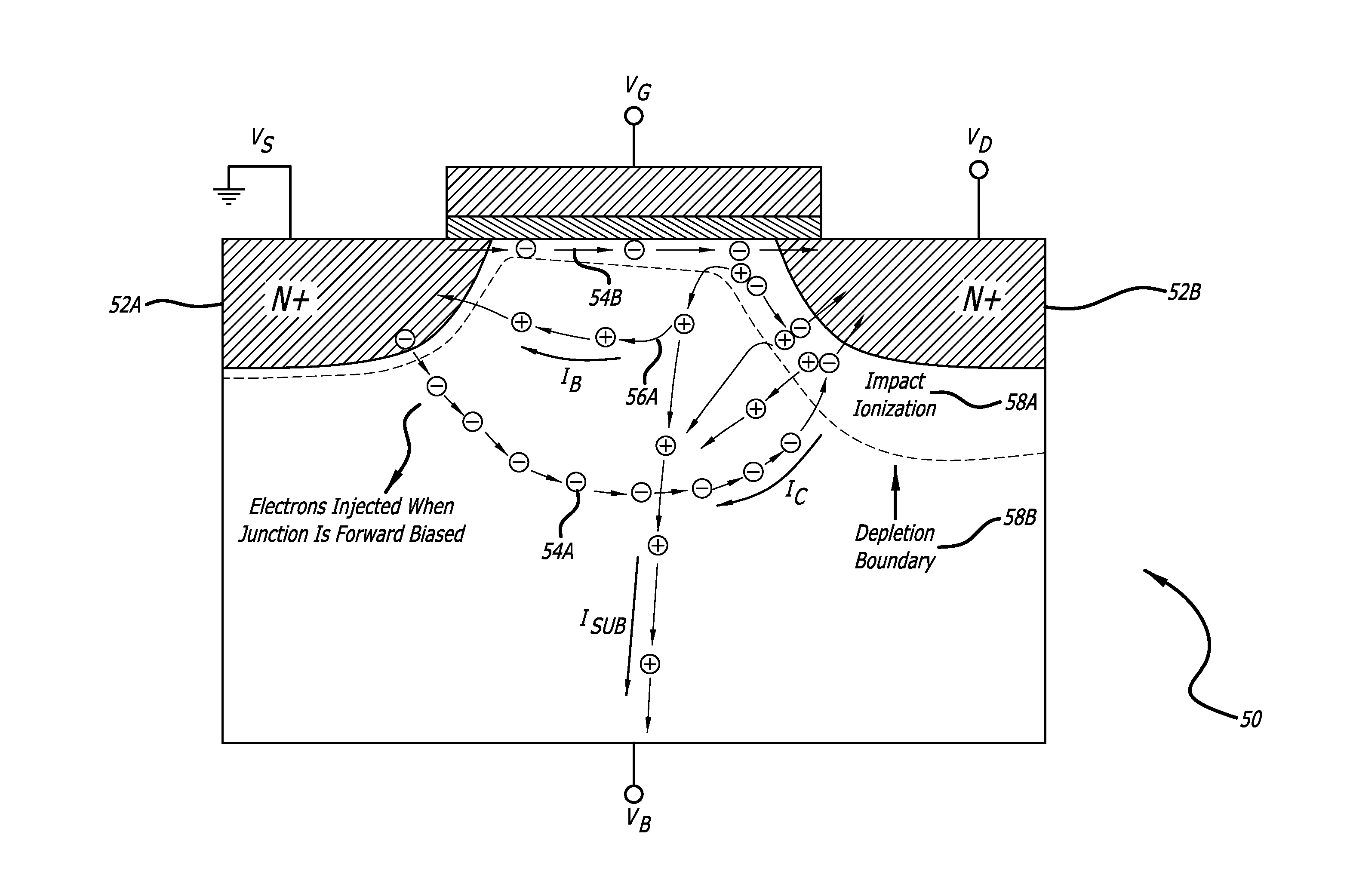
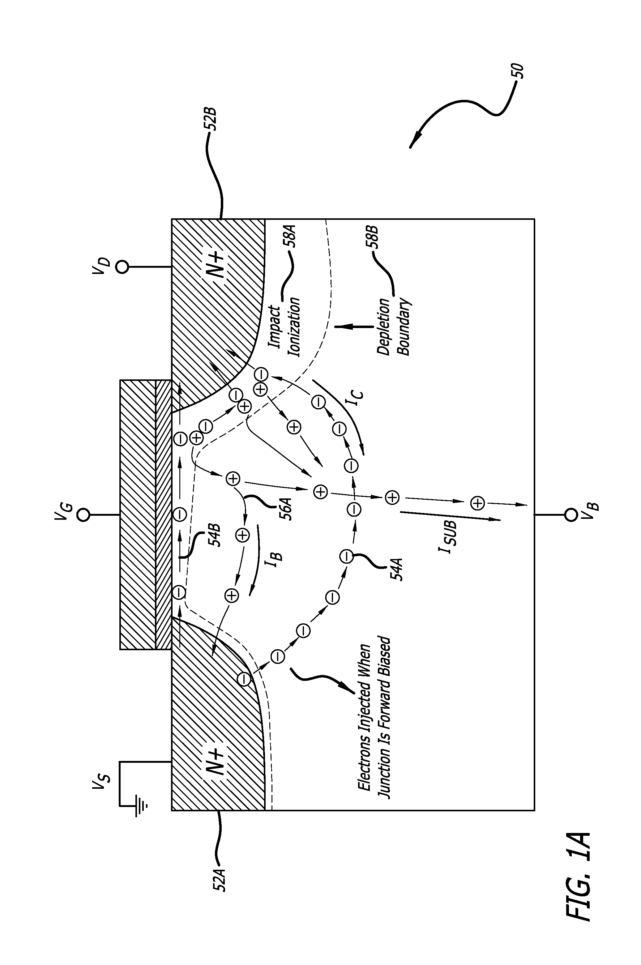
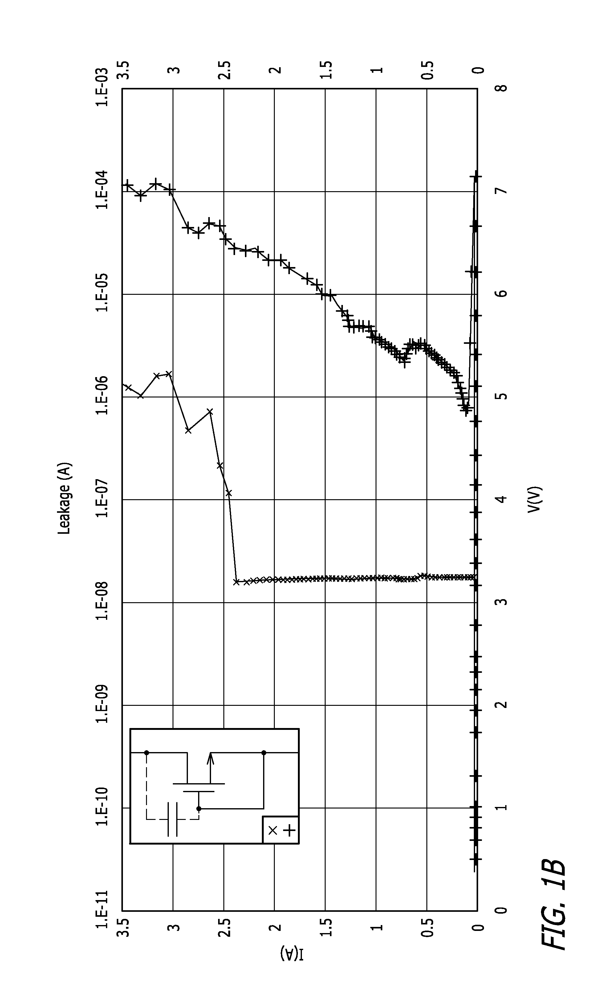
[0020]Integrated circuits (ICs) based on semiconductor devices can include electrostatic discharge (ESD) protection devices coupled to one or more pins of the ICs. Such ESD protection devices can include a semiconductor device (e.g. transistor) configured, during an ESD event, to conduct high transient currents resulting from discharge of electrostatic energy accumulated on a human body or on a machine or within the ICs. Energy from such electrostatic discharge events may be required or desired to be processed by the ESD protection devices without operatively damaging the ICs. System standards or specifications may require the IC, via its ESD protection devices,...


PUM


Abstract

Systems, methods, and apparatus for ESD protection with adjustable trigger voltage decoupled from DC breakdown voltage for semiconductor devices including field effect transistors (FETs), and particularly to metal-oxide-semiconductors (MOSFETs) fabricated on silicon-on-insulator (“SOI”) and silicon-on-sapphire (“SOS”) substrates are described. The apparatus and method are configured to change reverse biased drain junctions which in turn can control the DC breakdown voltage and the trigger voltage.

Description

TECHNICAL FIELD[0001]Various embodiments described herein relate generally to systems, methods, and apparatus for improving electrostatic discharge (ESD) performance for semiconductor devices.BACKGROUND[0002]It may be desirable to improve ESD performance for semiconductor devices used as ESD protection elements in radio frequency (RF) integrated circuits (ICs). Such semiconductor devices can include metal-oxide-semiconductor (MOS) field effect transistors (FETs), and particularly to MOSFETs fabricated on silicon-on-insulator (“SOI”) and silicon-on-sapphire (“SOS”) substrates.SUMMARY[0003]According to a first aspect of the present disclosure, an electrostatic discharge (ESD) protection device comprising a multiple fingers field-effect transistor (FET) is presented, the ESD protection device being configured to exhibit, during operation, a trigger voltage and a direct current breakdown voltage, wherein a finger of the multiple fingers FET comprises: a drain implantation region and cor...

Claims


Application Information

Patent Timeline
Patent Type & Authority Applications(United States)
IPC IPC(8): H02H9/04H01L27/02
CPCH01L27/0266H02H9/04H01L27/027
Inventor KUSHNER, VADIMPOOLE, ERICA
Owner PSEMI CORP
Why Eureka
Try Eureka