Semiconductor device and method of forming the same

a technology of semiconductor devices and metal gate structures, applied in the direction of semiconductor devices, electrical devices, transistors, etc., can solve the problems of inferior performance, gate capacitance reduction, and conventional poly-silicon gate faces, and achieve the effect of improving the substrate

Active Publication Date: 2016-09-22
UNITED MICROELECTRONICS CORP
View PDF7 Cites 25 Cited by
  • Summary
  • Abstract
  • Description
  • Claims
  • Application Information

AI Technical Summary

Benefits of technology

[0011]The semiconductor device and the forming method thereof in the present invention utilizes forming stacked work function layers with different work functions (for example, work function layers having different materials, different thicknesses or different bondings) and performing different threshold voltage implantation processes, to adjust the threshold voltage of each transistor region. Through such performances, the gate structures formed subsequently in each transistor region may be able to achieve different threshold voltages, thereby improving the substrate effect and forming metal gate structures with different threshold voltages.

Problems solved by technology

With the trend towards scaling down the size of semiconductor devices, however, conventional poly-silicon gates face problems such as inferior performance due to boron penetration and unavoidable depletion effect.
This increases equivalent thickness of the gate dielectric layer, reduces gate capacitance, and worsens a driving force of the devices.
Nevertheless, threshold voltages in current finFETs cannot be easily adjusted by using ion implantation.

Method used


Image

  • Semiconductor device and method of forming the same
  • Semiconductor device and method of forming the same
  • Semiconductor device and method of forming the same

Examples


Embodiment Construction

[0017]To provide a better understanding of the present invention, preferred embodiments will be described in detail. The preferred embodiments of the present invention are illustrated in the accompanying drawings with numbered elements.

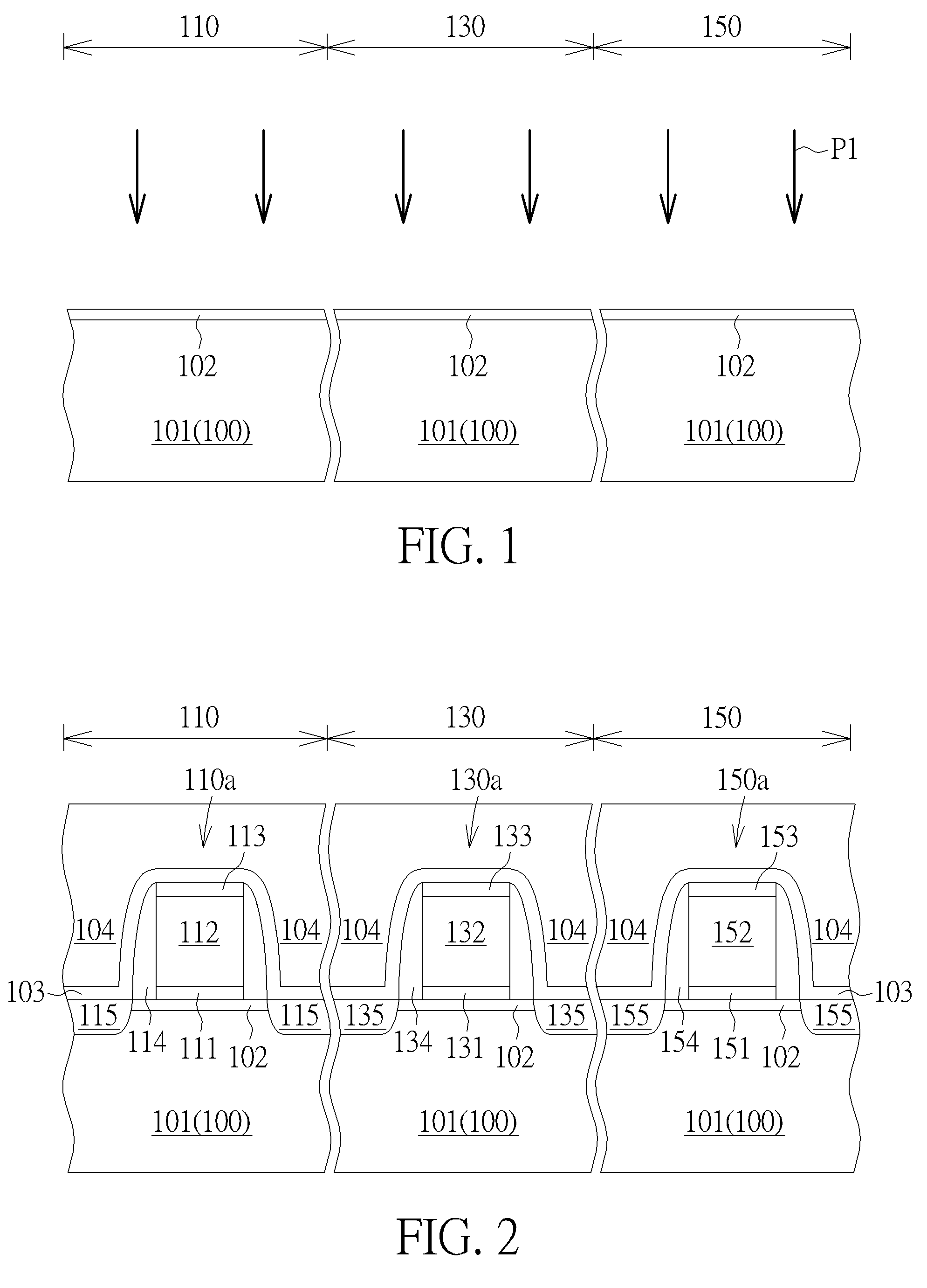
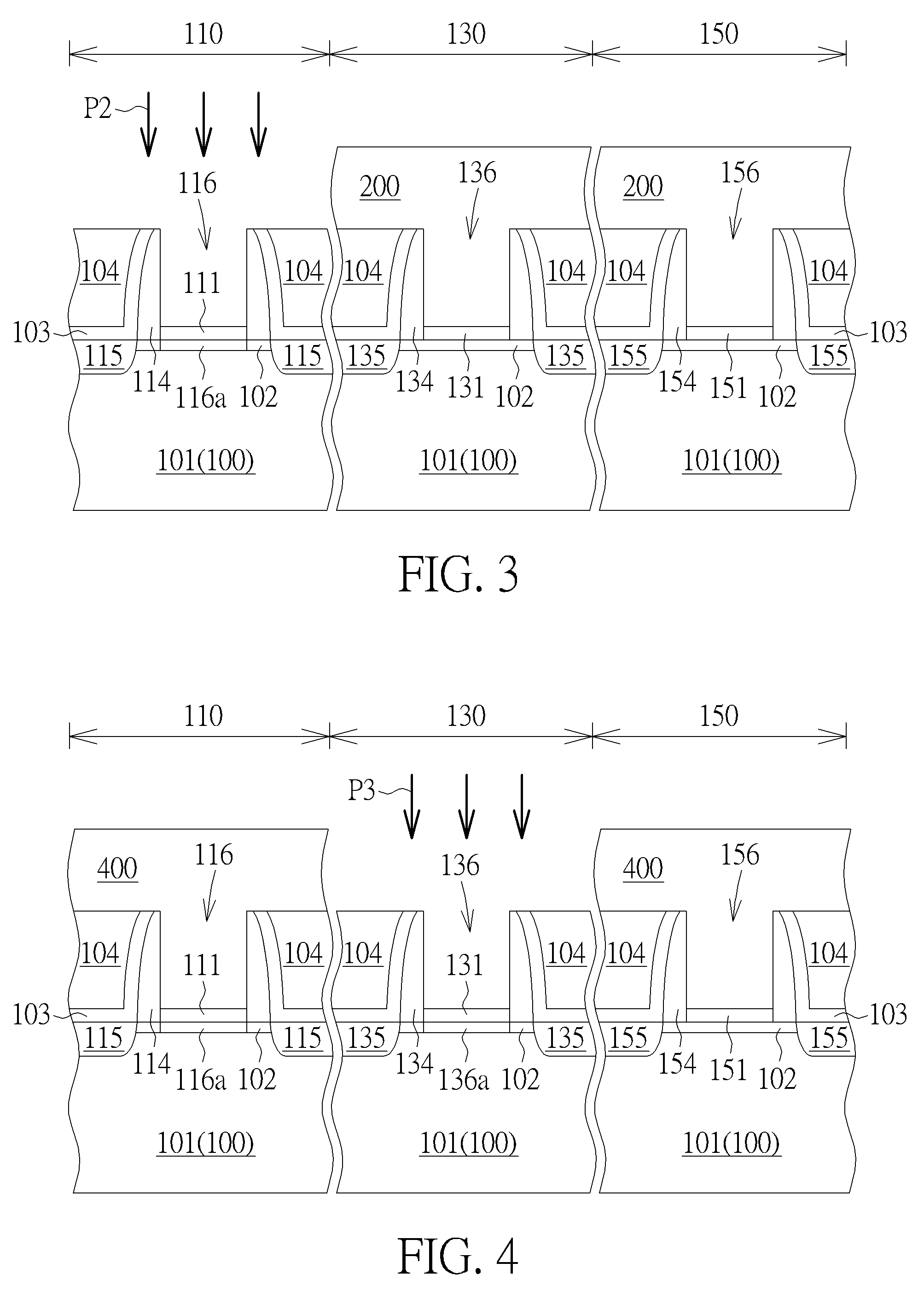
[0018]Please refer to FIG. 1 to FIG. 5, which are schematic diagrams illustrating a method of forming a semiconductor device according to the first embodiment of the present invention. First of all, as shown in FIG. 1, a substrate 100 is provided. The substrate 100 for example includes a semiconductor substrate, such as a silicon substrate, a silicon-containing substrate or a silicon-on-insulator (SOI) substrate. Then, three transistor regions 110, 130, 150 are defined on the substrate 100. The three transistor regions 110, 130, 150 are preferably composed of a same conductive type, such as PMOS regions or NMOS regions, and the three transistor regions 110, 130, 150 are configured to fabricate gate structures having different threshold voltages afterw...


PUM


Abstract

The present invention provides a semiconductor device and a method of forming the same. The semiconductor device includes a substrate, a first transistor and a second transistor. The first transistor and the second transistor are disposed on the substrate. The first transistor includes a first channel and a first work function layer. The second transistor includes a second channel and a second work function layer, where the first channel and the second channel include different dopants, and the second work function layer and the first work function layer have a same conductive type and different thicknesses.

Description

BACKGROUND OF THE INVENTION[0001]1. Field of the Invention[0002]The invention relates to a semiconductor process of forming a metal gate structure with different threshold voltages and a semiconductor device thereof, and more specifically to a semiconductor process of forming a metal gate structure with different threshold voltages by applying stacked work function layers and performing different threshold voltage implantation processes, and a semiconductor device thereof.[0003]2. Description of the Prior Art[0004]Poly-silicon is conventionally used as a gate electrode in semiconductor devices, such as the metal-oxide-semiconductor (MOS). With the trend towards scaling down the size of semiconductor devices, however, conventional poly-silicon gates face problems such as inferior performance due to boron penetration and unavoidable depletion effect. This increases equivalent thickness of the gate dielectric layer, reduces gate capacitance, and worsens a driving force of the devices. ...

Claims


Application Information

Patent Timeline
Patent Type & Authority Applications(United States)
IPC IPC(8): H01L21/8238H01L21/265H01L27/092H01L29/66
CPCH01L21/823842H01L29/66545H01L21/82385H01L27/0924H01L21/26513H01L27/0922H01L21/823821H01L29/66537H01L27/092H01L21/82345
Inventor GAN, TIAN CHOYHSIAO, CHU-YUNHSU, CHIA-FU
Owner UNITED MICROELECTRONICS CORP
Why Eureka
Try Eureka