

Organic Light Emitting Device, Manufacturing Method Thereof and Display Device
- Summary
- Abstract
- Description
- Claims
- Application Information
AI Technical Summary
Benefits of technology
Problems solved by technology
Method used
Image

Examples
embodiment 1
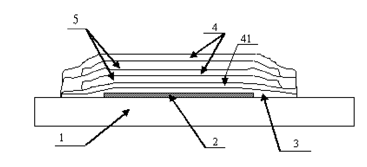
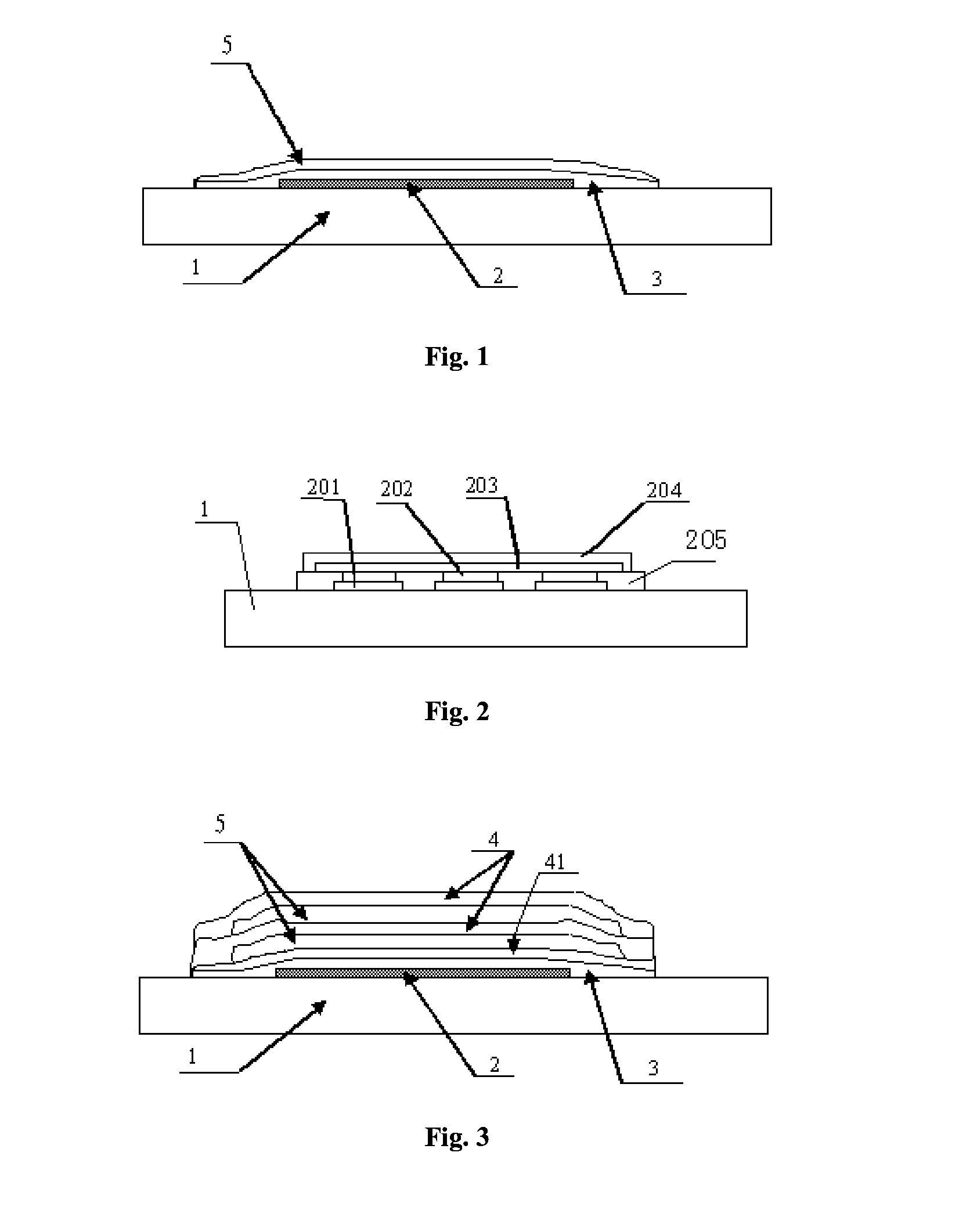
[0034]As shown in FIG. 3, this embodiment provides an organic light emitting device, including a substrate 1, an organic light emitting unit 2 arranged on the substrate 1 and a pre-encapsulation layer 3 covering the organic light emitting unit 2; wherein a first inorganic thin film 41 is arranged on the pre-encapsulation layer 3.
[0035]The first inorganic thin film 41 has a denser molecular structure compared with the pre-encapsulation layer 3, for example, the first inorganic thin film can be formed at higher power (for example, deposition power). The first inorganic thin film 41 entirely covers the pre-encapsulation layer 3 and the organic light emitting unit 2 to prevent water and oxygen from invading the organic light emitting unit 2 via the pre-encapsulation layer 3 to influence the service life of the organic light emitting unit 2.
[0036]Preferably, at least one thin film group is sequentially arranged on the first inorganic thin film 41, and each thin film group is composed of ...
embodiment 2
[0046]This embodiment provides a manufacturing method of the above-mentioned organic light emitting device, including the following steps:[0047]1) forming a pre-encapsulation layer 3 on an organic light emitting unit 2 arranged on a substrate 1;[0048]2) forming a first inorganic thin film 41 on the pre-encapsulation layer 3; and[0049]3) sequentially forming an organic thin film 5 and an inorganic thin film 4 forming a thin film group on the first inorganic thin film 41.
[0050]Specifically, the manufacturing method of the organic light emitting device further includes the following steps:
[0051]A. preparing the organic light emitting unit on the substrate;[0052]a first electrode 201 and an organic functional layer 202 of the organic light emitting unit 2 are formed on the substrate 1; an insulating layer 205 is formed between the first electrode 201 and the organic functional layer 202; a second electrode 203 is formed on the organic functional layer 202 and the insulating layer 205, a...
PUM
 Abstract
Description
Claims
Application Information