Semiconductor module, method for manufacturing the same and power conversion apparatus

Active Publication Date: 2019-05-30
MITSUBISHI ELECTRIC CORP
View PDF4 Cites 0 Cited by
  • Summary
  • Abstract
  • Description
  • Claims
  • Application Information

AI Technical Summary

Benefits of technology

[0003]When devices using a semiconductor module are operated at high altitudes, an atmospheric pressure is likely to drop. This causes bubbles in the silicone gel, producing partial discharge inside the module depending on the bubble generating area, which may shorten the service life of the module. Particularly when bubbles are generated in silicone gel at an eaves part below a ceramic substrate, part

Problems solved by technology

When devices using a semiconductor module are operated at high altitudes, an atmospheric pressure is likely to drop.
This causes bubbles in the silicone gel, producing partial discharge inside the module depending on the bubble generating area, which may shorten the service life of the module.
Even when not used at high altitudes, bubbles are likely to accumulate in the eaves part due to degassing from a brazing material or solder of the ceramic substrate during assembly.
The bubbles below t

Method used


Image

  • Semiconductor module, method for manufacturing the same and power conversion apparatus
  • Semiconductor module, method for manufacturing the same and power conversion apparatus

Examples


Example

First Embodiment

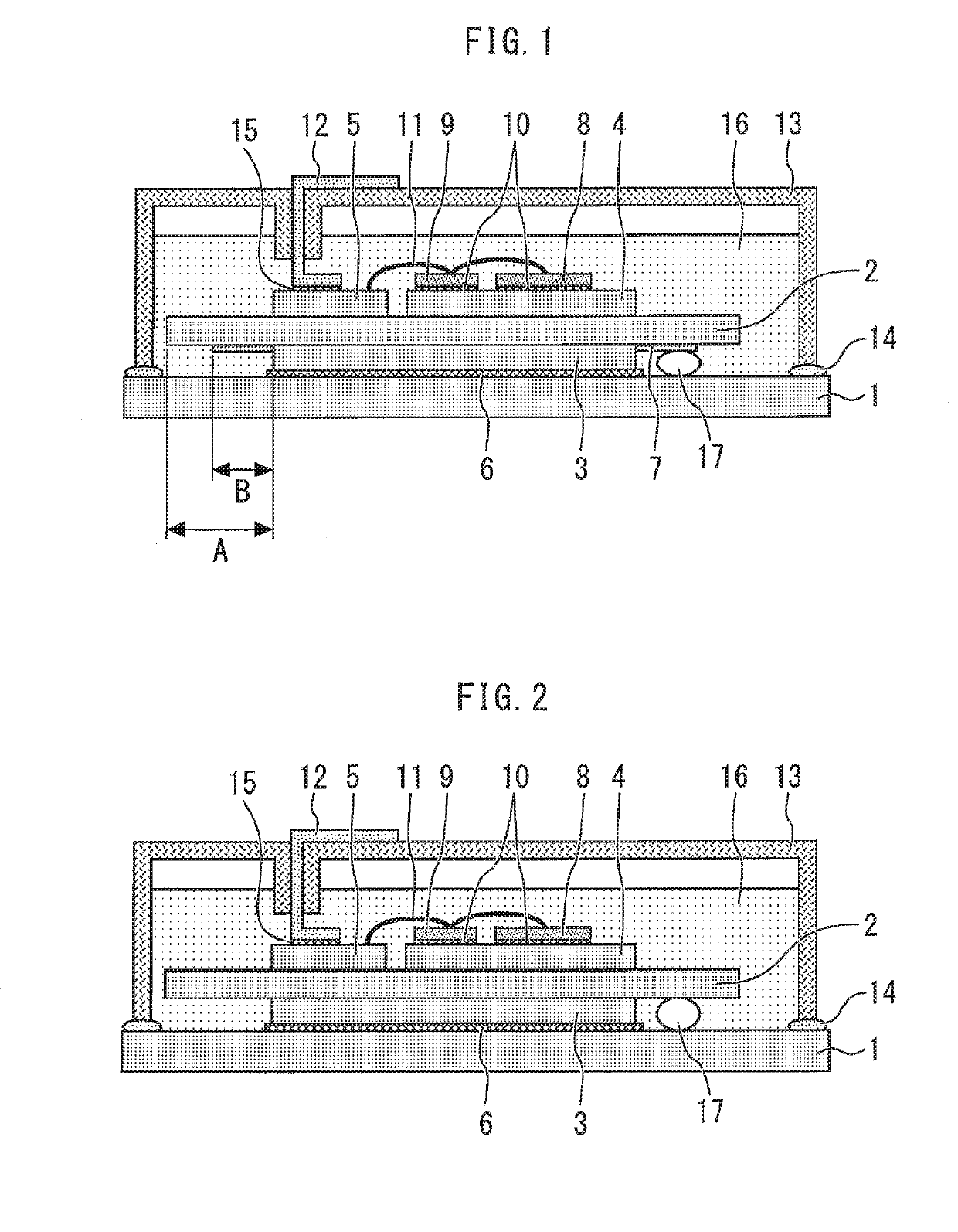
[0014]FIG. 1 is a cross-sectional view illustrating a semiconductor module according to a first embodiment. A ceramic substrate 2 is provided on a cooling base plate 1. The ceramic substrate 2 is made of, for example, silicon nitride or aluminum nitride and has a thickness of 200 μm to 1.2 mm.

[0015]An undersurface electrode 3, and top surface electrodes 4 and 5 are bonded to an undersurface and a top surface of the ceramic substrate 2 respectively using a brazing material such as Ag. A desired pattern is formed through a photoengraving process and the top surface electrodes 4 and 5 are patterned through selective etching using an etchant such as an acid. The undersurface electrode 3 and the top surface electrodes 4 and 5 are made of metal such as copper. The undersurface electrode 3 is bonded to the base plate 1 via solder 6. The top surface electrodes 4 and 5 on the substrate top surface need to have a thickness on the order of 200 to 500 μm to allow a high current ...

Example

Second Embodiment

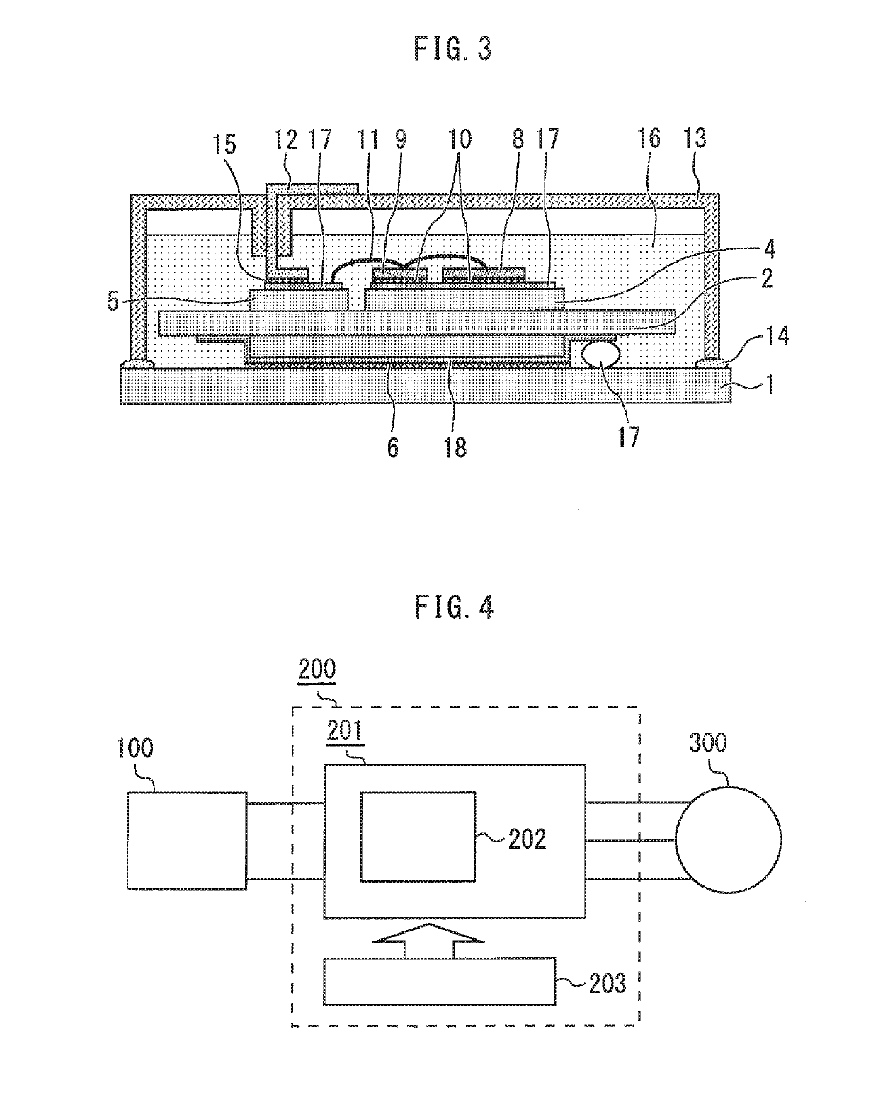
[0026]FIG. 3 is a cross-sectional view illustrating a semiconductor module according to a second embodiment. In order to secure solderability necessary in posterior steps, an electroless nickel plating layer 18 is selectively formed on the surfaces of the undersurface electrode 3 and the top surface electrodes 4 and 5. In that case, the electroless nickel plating layer 18 is also formed on the undersurface of the ceramic substrate 2, and by patterning the electroless nickel plating layer 18, it is possible to form the conductive thin-film 7. In addition, it is possible to obtain effects similar to the effects of the first embodiment.

[0027]Note that the conductive thin-film 7 is not limited to electroless nickel plating, but may be formed using metal such as nickel, tin or solder through an electron beam vapor deposition or sputtering apparatus. In this case, when a work is set in an electron beam vapor deposition apparatus, the conductive thin-film 7 is selectively ...

Example

Third Embodiment

[0034]In this embodiment, the semiconductor modules according to the first or second embodiment described above are applied to an electric power conversion device. The electric power conversion device is, for example, an inverter device, a converter device, a servo amplifier, or a power supply unit. Although the present invention is not limited to a specific electric power conversion device, a case where the present invention is applied to a three-phase inverter will be described below.

[0035]FIG. 4 is a block diagram illustrating a configuration of an electric power conversion system to which the electric power conversion device according to the third embodiment is applied. This electric power conversion system includes a power supply 100, an electric power conversion device 200, and a load 300. The power supply 100 is a DC power supply and supplies DC power to the electric power conversion device 200. The power supply 100 can be composed of various components. For e...


PUM


Abstract

A conductive thin-film thinner than the undersurface electrode is provided outside the undersurface electrode on the undersurface of the ceramic substrate and connected to the undersurface electrode. A length from an outer circumferential part of the undersurface electrode to an outer circumferential pert of the ceramic substrate is equal to a length from an outer circumferential part of the top surface electrode to an outer circumferential part of the ceramic substrate. A thickness of the conductive thin-film is half or less than a thickness of the ceramic substrate.

Description

BACKGROUND OF THE INVENTIONField[0001]The present invention relates to a semiconductor module, a method for manufacturing the same and a power conversion apparatus.Background[0002]Semiconductor modules are used to control motors for industrial equipment and electric railways or the like. Silicone gel is used as an insulation sealing material for semiconductor modules (e.g., see FIG. 20 in WO 2016 / 098431 A).SUMMARY[0003]When devices using a semiconductor module are operated at high altitudes, an atmospheric pressure is likely to drop. This causes bubbles in the silicone gel, producing partial discharge inside the module depending on the bubble generating area, which may shorten the service life of the module. Particularly when bubbles are generated in silicone gel at an eaves part below a ceramic substrate, partial discharge is more likely to occur even at a low voltage. Even when not used at high altitudes, bubbles are likely to accumulate in the eaves part due to degassing from a b...

Claims


Application Information

Patent Timeline
IPC IPC(8): H01L23/498H01L25/07H01L23/15H01L23/31H01L21/48H02M7/00H02M7/537
CPCH01L23/49872H01L25/072H01L23/15H01L23/3121H01L23/49861H01L21/4807H01L21/4875H02M7/003H02M7/537H01L2224/32225H01L2224/48137H01L2224/48227H01L2224/73265H01L23/3735H01L23/49866H01L23/053H01L23/24H01L23/49811H01L23/62H01L2924/16151H01L2924/16152H01L2924/181H01L2924/00012H01L2924/00
Inventor TANAKA, YASUO
Owner MITSUBISHI ELECTRIC CORP
Why Eureka
Try Eureka