Output stage circuit

Active Publication Date: 2021-10-14
VIA ALLIANCE SEMICON CO LTD
View PDF0 Cites 2 Cited by
  • Summary
  • Abstract
  • Description
  • Claims
  • Application Information

AI Technical Summary

Benefits of technology

[0005]The invention is directed to an output stage circuit, the output stage circuit dynamically adjusts a bias voltage according to a value of an output voltage, so that three-terminal voltages of each tran

Problems solved by technology

However, when the output stage circuit is actually used, since there must be a phenomenon of voltage overshoot of the input/output signal, the withstand voltages of some components of the output stage

Method used


Image

  • Output stage circuit
  • Output stage circuit
  • Output stage circuit

Examples


Example

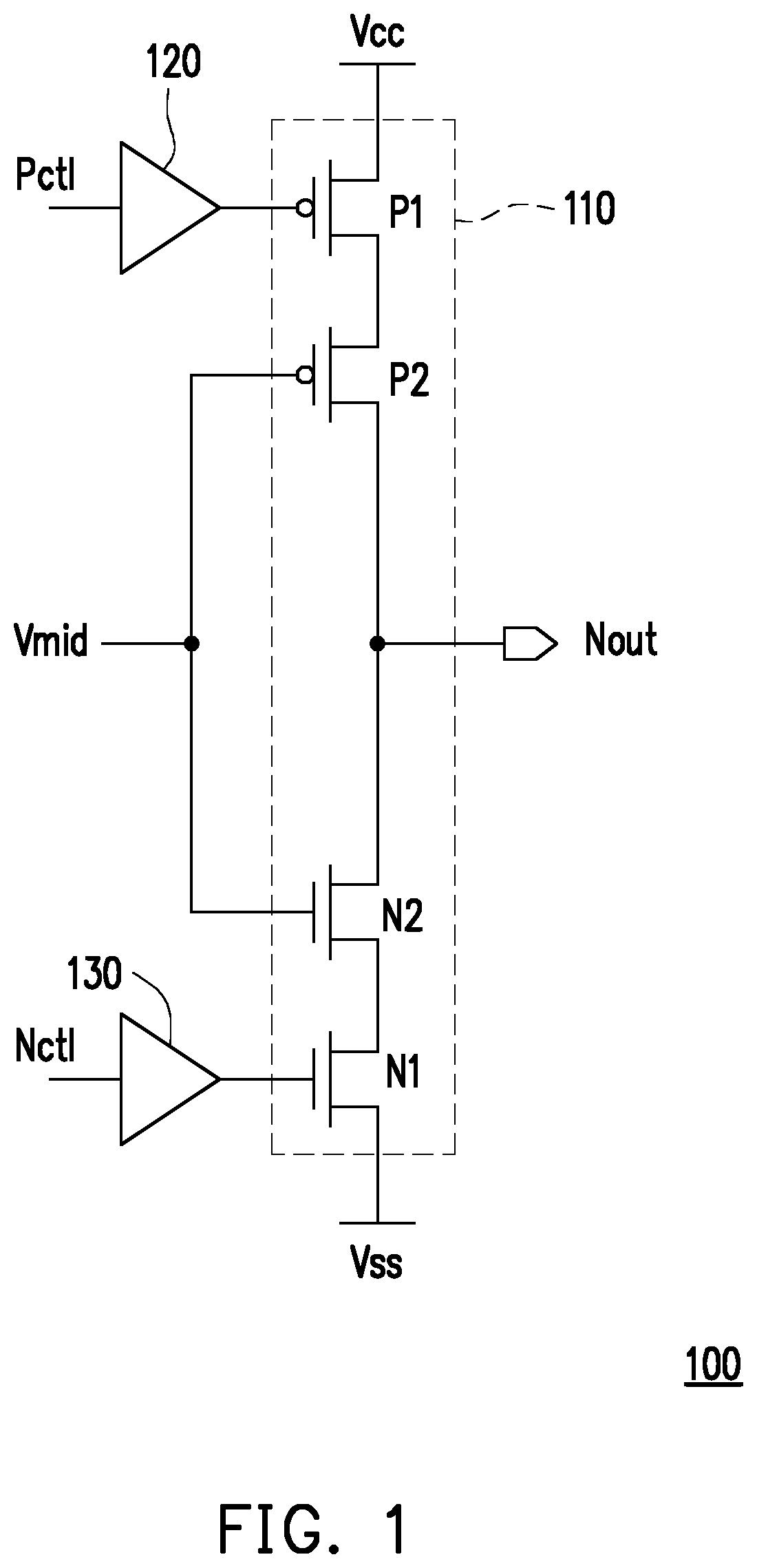
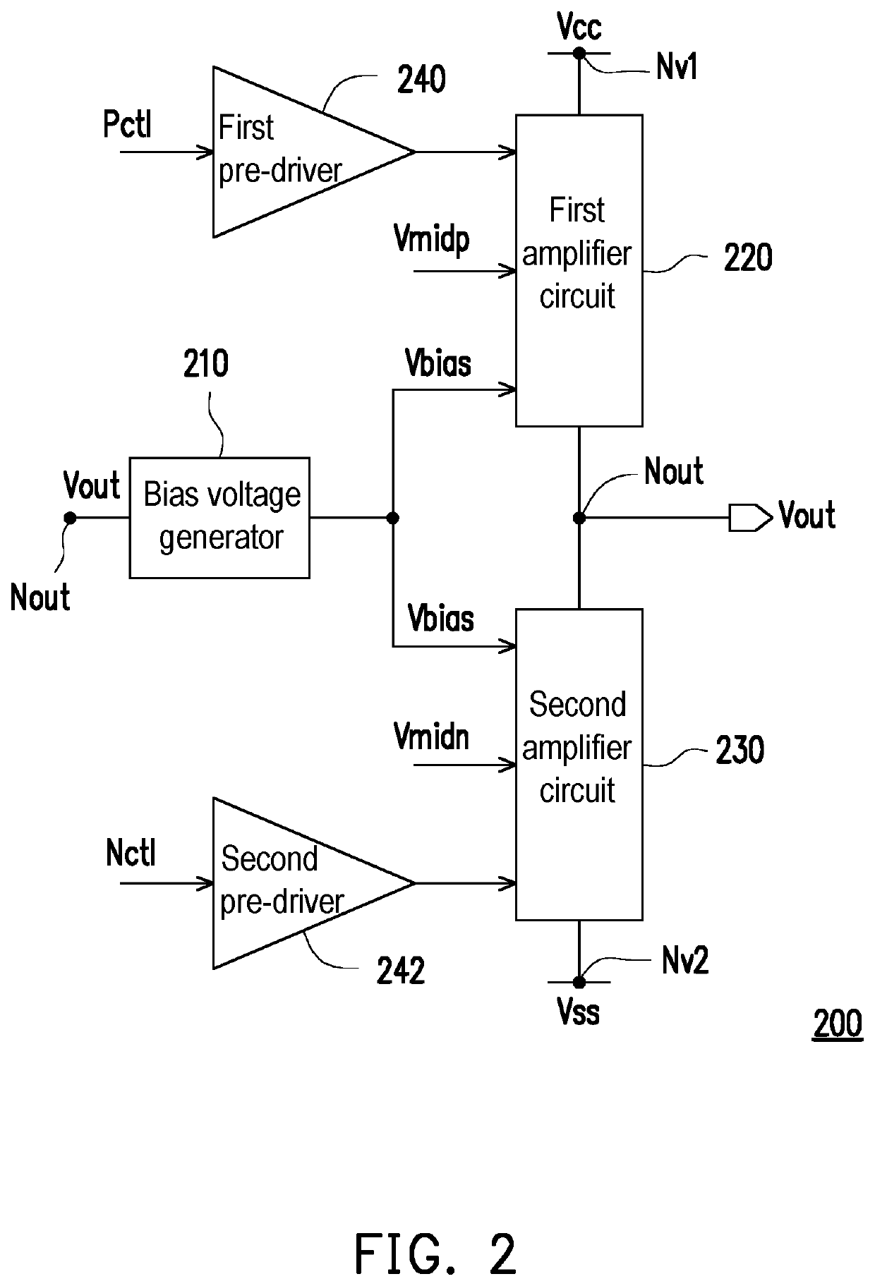
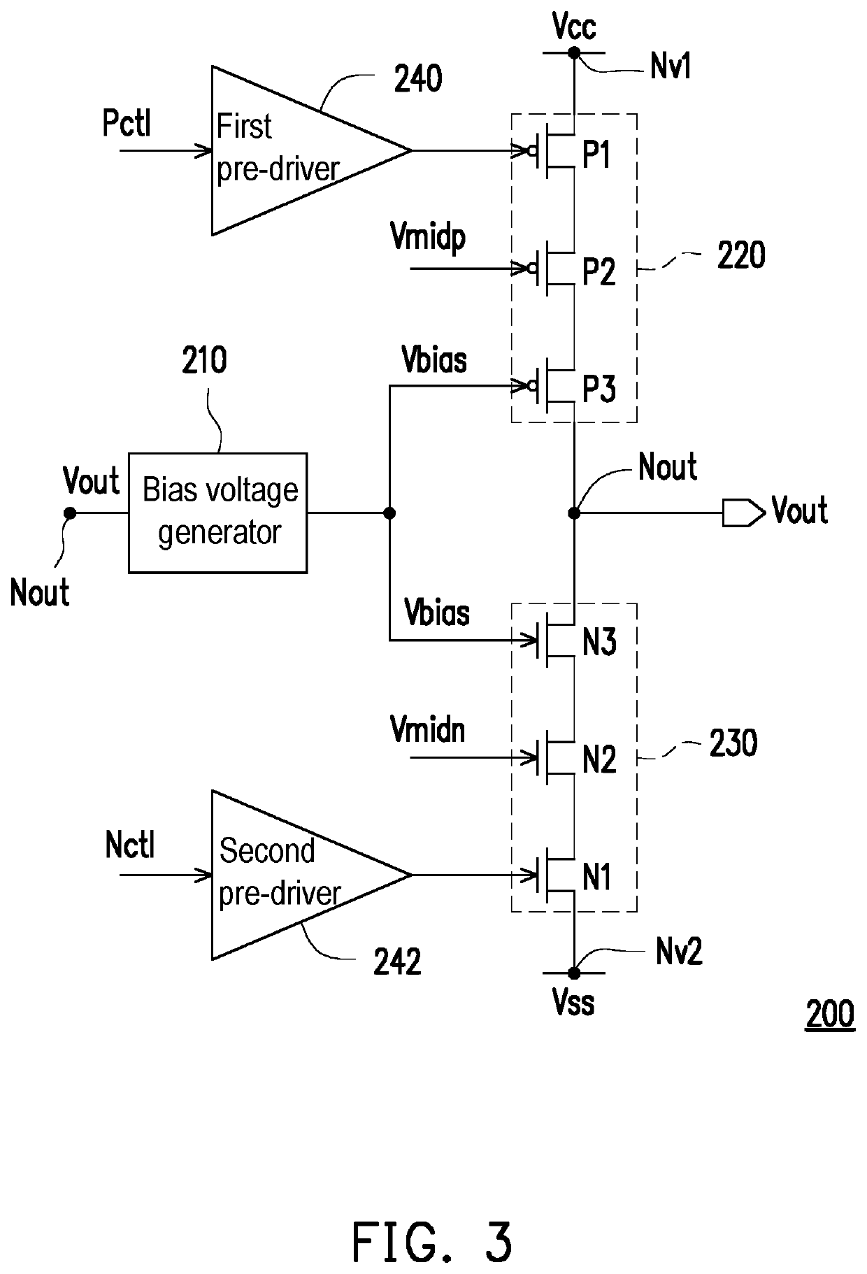
[0015]FIG. 1 is a circuit diagram of an output stage circuit 100. The output stage circuit 100 in FIG. 1 comprises a two-tier amplifier circuit 110 composed of transistors P1, P2, N1 and N2, and two pre-drivers 120 and 130. It is assumed that a withstand voltage of each transistor of the output stage circuit 100 is 1.8V due to limitation of a semiconductor process, and a chip using the output stage circuit 100 needs to transmit a data signal with a maximum voltage of 3.3V at an output terminal Nout of the output stage circuit 100 due to a transmission protocol of a specific interface. The transistors P1 and P2 of the embodiment are both P-type metal-oxide-semiconductor field-effect transistors (MOSFETs), and the transistors N1 and N2 are both N-type MOSFETs.

[0016]The pre-driver 120 receives a first control signal Pctl and pre-drives the first control signal Pctl, and transmits the pre-driven first control signal Pctl to a control terminal (a gate) of the transistor P1. The pre-drive...


PUM


Abstract

An output stage circuit comprising a bias voltage generator, a first amplifier circuit and a second amplifier circuit is provided. The bias voltage generator is coupled to an output terminal of the output stage circuit to generate a bias voltage according to an output voltage of the output terminal. The first amplifier circuit is coupled to the output terminal, a first power supply terminal and the bias voltage generator, receives a first pre-driving signal, a first predetermined voltage and the bias voltage, and determines whether to transmit a first voltage to serve as the output voltage. The second amplifier circuit is coupled to the output terminal, a second power supply terminal and the bias voltage generator, receives a second pre-driving signal, a second predetermined voltage and the bias voltage, and determines whether to transmit a second voltage to serve as the output voltage.

Description

CROSS-REFERENCE TO RELATED APPLICATION[0001]This application claims the priority benefit of China application no. 202010278121.8, filed on Apr. 10, 2020. The entirety of the above-mentioned patent application is hereby incorporated by reference herein and made a part of this specification.BACKGROUNDTechnical Field[0002]The disclosure relates to an output stage circuit, and particularly relates to an output stage circuit capable of avoiding or reducing damage resulting from voltage overshoot.Description of Related Art[0003]When the structure of a chip is designed, characteristics of manufactured components may be different due to different semiconductor processes. For example, transistors produced by different semiconductor processes may have different voltage withstand levels. In addition, based on technical specifications and application limitations and advances in semiconductor technology, an input / output signal voltage used in a currently circuit is designed in accordance with ru...

Claims


Application Information

Patent Timeline
IPC IPC(8): H03F3/16H03K5/24
CPCH03F3/16H03K5/24H03F1/523H03F3/68H03F3/2173H03F1/0272
Inventor LI, SHENLIU, ZHONGDING
Owner VIA ALLIANCE SEMICON CO LTD
Why Eureka
Try Eureka