Memory device and method of manufacturing the same

a memory device and manufacturing method technology, applied in the field of memory devices and manufacturing methods, can solve problems such as micro-loading effect, difficulty in the window of subsequent processes, and errors in the size of semiconductor devices, and achieve the effect of improving a sub-trench defect of the peripheral circuit region

Active Publication Date: 2016-09-29
MACRONIX INT CO LTD
View PDF1 Cites 6 Cited by
  • Summary
  • Abstract
  • Description
  • Claims
  • Application Information

AI Technical Summary

Benefits of technology

[0005]The invention provides a memory device and a method of manufacturing the same for solving a micro-loading effect between

Problems solved by technology

However, due to the increasing aspect ratio of the memory device, the different pattern densities of the memory cell array region and the peripheral circuit region may easily cause the micro-loading effect.
The micro-loading effect generally refers to errors of the size of the

Method used


Image

  • Memory device and method of manufacturing the same
  • Memory device and method of manufacturing the same
  • Memory device and method of manufacturing the same

Examples


Embodiment Construction

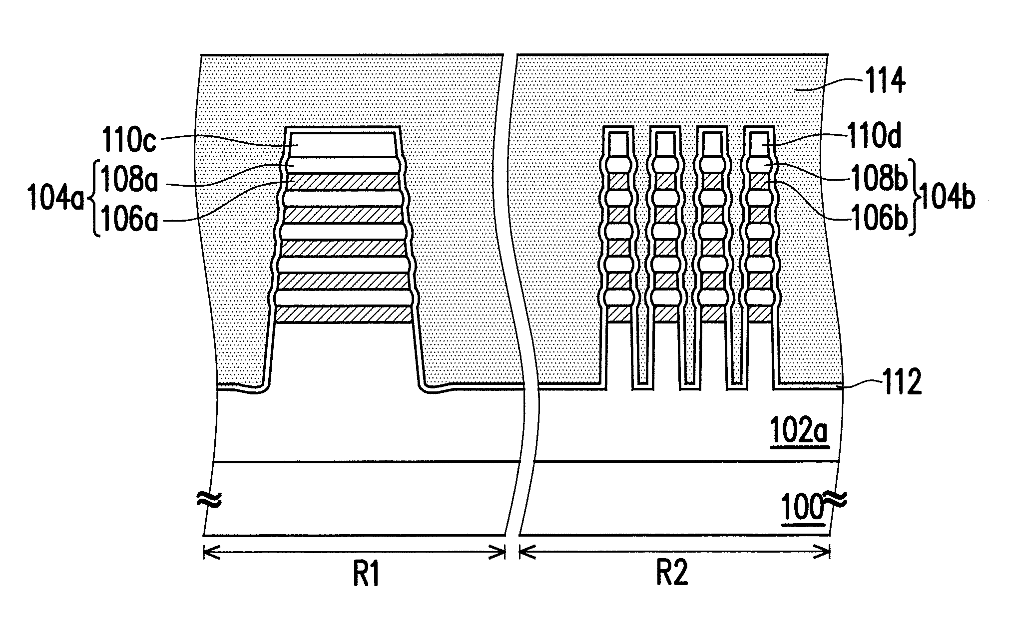
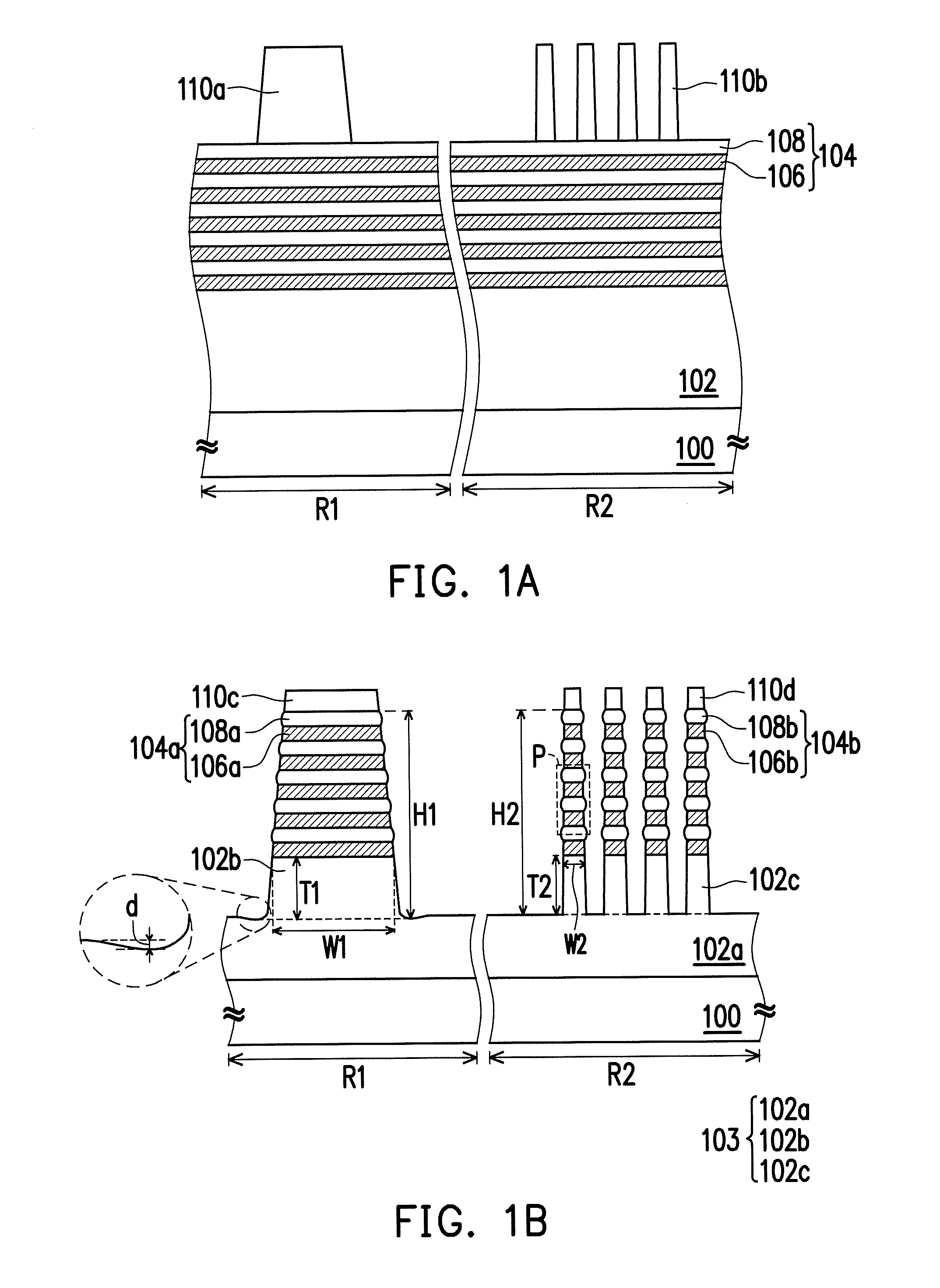
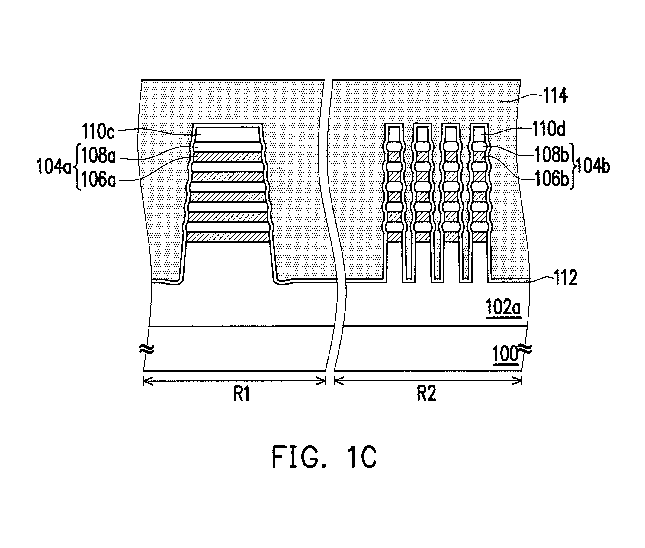
[0031]FIG. 1A to FIG. 1C are schematic cross-sectional views showing a manufacturing method of a memory device according to an embodiment of the invention.

[0032]With reference to FIG. 1A, first, a substrate 100 is provided. The substrate 100 has a first region R1 and a second region R2. In this embodiment, the first region R1 is a peripheral circuit region and the second region R2 is a memory cell array region, for example. The substrate 100 is a semiconductor substrate, a semiconductor compound substrate, or a semiconductor over insulator (SOI) substrate, for example. The semiconductor is IVA group atoms, such as silicon or germanium, for example. The semiconductor compound is forming of IVA group atoms, such as silicon carbide or silicon germanium, or formed of IIIA group atoms and VA group atoms, such as gallium arsenide, for example.

[0033]Then, a bottom dielectric layer 102 is formed on the substrate 100. The bottom dielectric layer 102 is disposed across the first region R1 and...


PUM


Abstract

Provided is a memory device including a substrate, a first stack structure, and a plurality of second stack structures. The substrate has a first region and a second region. The first stack structure is located on the substrate of the first region. The second stack structures are located on the substrate of the second region. A sidewall of the first stack structure and a sidewall of the second stack structure have a concave-and-convex surface respectively.

Description

BACKGROUND OF THE INVENTION[0001]1. Field of the Invention[0002]The invention relates to a semiconductor device and a method of manufacturing the same, and more particularly relates to a memory device and a method of manufacturing the same.[0003]2. Description of Related Art[0004]With the advancement of technology, it has become a trend to integrate components of the memory cell array region and the peripheral circuit region on the same chip in order to reduce costs, simplify manufacturing steps, and save the chip area. However, due to the increasing aspect ratio of the memory device, the different pattern densities of the memory cell array region and the peripheral circuit region may easily cause the micro-loading effect. The micro-loading effect generally refers to errors of the size of the semiconductor device that occur during the etching process due to the different pattern densities. For example, the peripheral circuit region where the pattern density is lower may easily have ...

Claims


Application Information

Patent Timeline
IPC IPC(8): H01L29/423H01L27/115
CPCH01L29/42372H01L29/42364H01L27/11582H10B43/35H10B43/50H10B43/40H10B43/27
Inventor YANG, ZU-SING
Owner MACRONIX INT CO LTD
Why Eureka
Try Eureka