Diode and method of manufacturing diode

Inactive Publication Date: 2016-10-13
TOYOTA JIDOSHA KK +1
View PDF2 Cites 5 Cited by
  • Summary
  • Abstract
  • Description
  • Claims
  • Application Information

AI Technical Summary

Benefits of technology

[0009]The diode comprises the p-type contact regions, including the first region having the high p-type impurity density, the second region having the medium p-type impurity density, and the third region having the low p-type impurity density. In the second region, the p-type impurity density is distributed within the range from minus 30% to plus 30%, meaning that a difference in the p-type impurity density is small. Further, the second region is thicker than the first region. That is, in this diode, the second region in which the p-type impurity density is distributed at a medium degree is thick. The first region having the high p-type impurity density is provided by making its barrier between the anode electrode and the p-type contact regions small so as to increase a response speed of the diode. When a reverse voltage is applied to this diode, a depletion layer spreads from the p-type contact regions to the n-type contact region, as a result of which the n-type contact region is pinched off. Here, the third region with the low p-type impurity density hardly contributes to the spreading of the depletion layer to the n-type contact region since the third region is instantly depleted, however, the first region having the high

Problems solved by technology

Further, if the p-type impurity density of the p-type contact regions is made low in order to suppress the electric field concentration, the p-type contact regions are depleted upon the application of the reverse voltage.
If the p-type contact regions are depleted, the depletion layer would not spread further into the n-type contact regions, as a result of which the pinch-off of the n-t

Method used


Image

  • Diode and method of manufacturing diode
  • Diode and method of manufacturing diode
  • Diode and method of manufacturing diode

Examples


Embodiment Construction

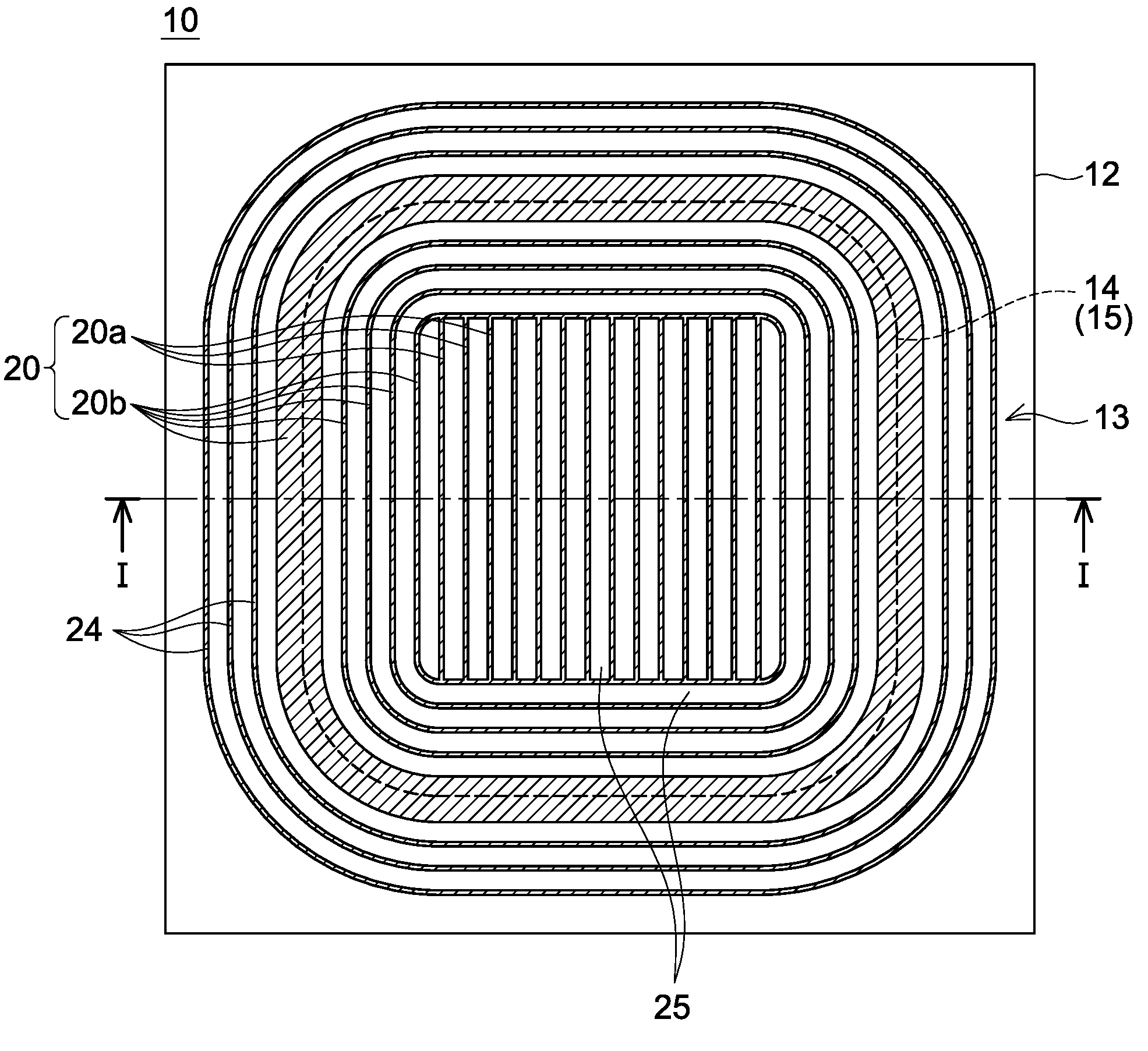
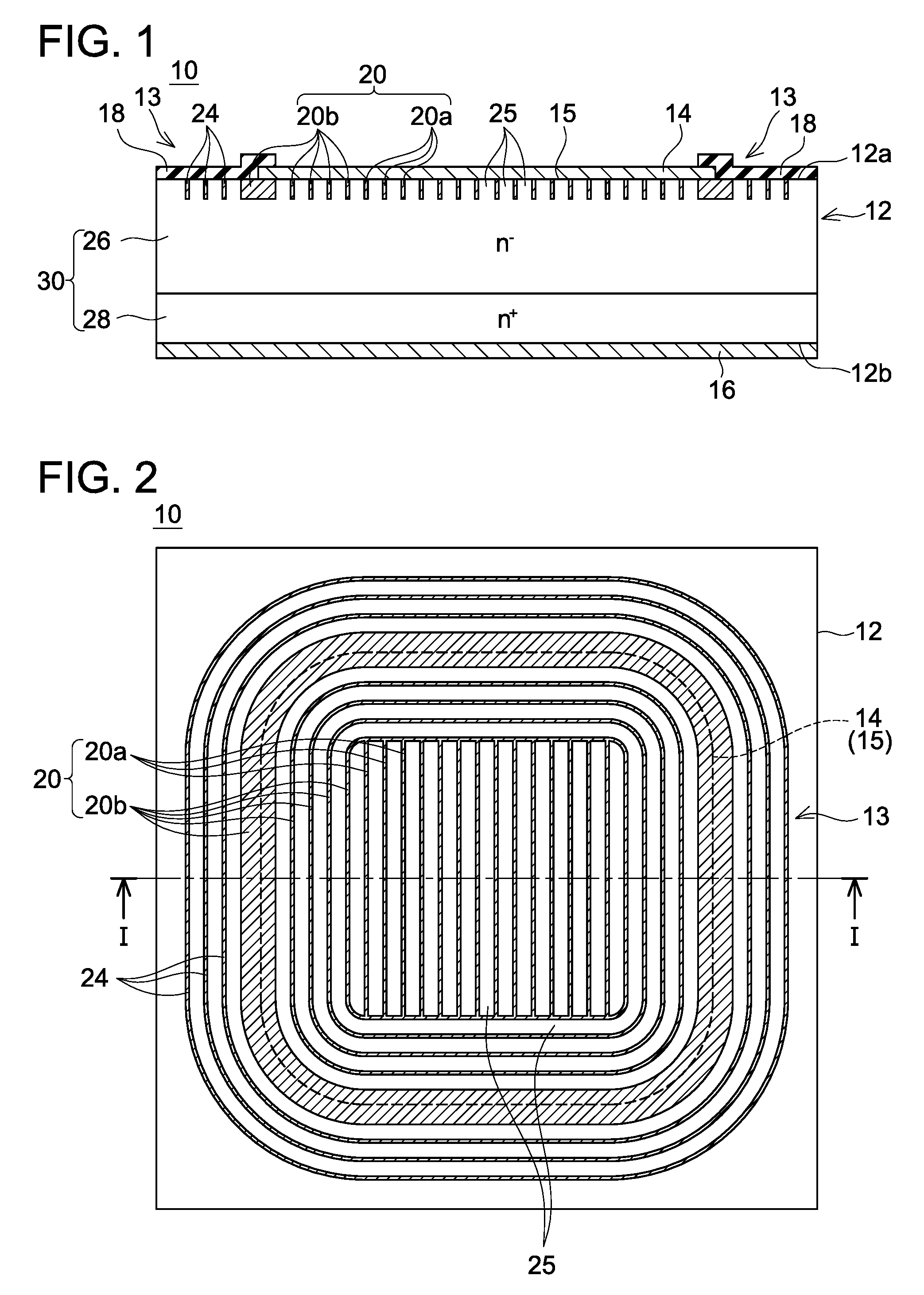
[0022]A diode 10 of an embodiment shown in FIGS. 1 and 2 comprises a semiconductor substrate 12. Notably in FIG. 2, a p-type region is shown by oblique hatched lines. The semiconductor substrate 12 is configured of a wide-gap semiconductor (e.g., SiC). An anode electrode 14 and an insulating film 18 are provided on a front surface 12a of the semiconductor substrate 12. A dotted line 14 in FIG. 2 shows a contour of a range where the anode electrode 14 is provided (i.e., a contact surface 15 where the semiconductor substrate 12 and the anode electrode 14 make contact). The anode electrode 14 is provided at a center portion of the front surface 12a of the semiconductor substrate 12. A region on the front surface 12a that is not covered by the anode electrode 14 (i.e., a region on an outer side of the dotted line 14; hereafter termed a peripheral region 13) is covered by the insulating film 18. A cathode electrode 16 is provided on a rear surface 12b of the semiconductor substrate 12.

[0...


PUM


Abstract

A diode is provided with a semiconductor substrate; an anode electrode located on a front surface of the semiconductor substrate; and a cathode electrode located on a rear surface of the semiconductor substrate. Each of the p-type contact regions includes: a first region being in contact with the anode electrode; a second region located on the rear surface side of the first region, having a p-type impurity density lower than a p-type impurity density in the first region; and a third region located on the rear surface side of the second region and having a p-type impurity density lower than the p-type impurity density in the second region. A thickness of the second region is thicker than a thickness of the first region.

Description

CROSS-REFERENCE TO RELATED APPLICATION[0001]This application claims priority to Japanese Patent Application No. 2015-080217 filed on Apr. 9, 2015, the entire contents of which are hereby incorporated by reference into the present application.TECHNICAL FIELD[0002]The technique disclosed in this disclosure relates to a diode and a method of manufacturing a diode.DESCRIPTION OF RELATED ART[0003]Japanese Patent Application Publication No. 2009-94433 discloses a diode provided with a plurality of p-type contact regions, n-type contact regions, and an n-type cathode region. Each n-type contact region is arranged between two p-type contact regions that are adjacent to each other. The p-type contact regions and the n-type contact regions make contact with an anode electrode. The cathode region is arranged on a rear surface side of the p-type contact regions and the n-type contact regions, and makes contact with a cathode electrode. An n-type impurity density of the n-type contact regions is...

Claims


Application Information

Patent Timeline
IPC IPC(8): H01L29/861H01L21/265H01L29/66
CPCH01L29/861H01L21/26513H01L29/66136H01L29/0607H01L29/0611H01L29/6609H01L29/6606H01L29/872H01L29/0619H01L29/0692H01L29/1608H01L29/0615
Inventor MIYAKE, HIROKINAGAOKA, TATSUJIMIYAHARA, SHINICHIROAOI, SACHIKO
Owner TOYOTA JIDOSHA KK
Why Eureka
Try Eureka