Biometric feature identification device and method

a biometric and feature identification technology, applied in the field of sensing devices, can solve the problems of unsatisfactory product life and tolerance, high material cost and packaging cost, etc., and achieve the effects of increasing sensing sensitivity and snr, increasing stability and correctness, and enhancing deflection signal

Active Publication Date: 2016-10-27
SUPERC TOUCH CORP
View PDF3 Cites 8 Cited by
  • Summary
  • Abstract
  • Description
  • Claims
  • Application Information

AI Technical Summary

Benefits of technology

[0007]The object of the present invention is to provide a biometric feature identification device, which uses a plurality of selection switches to divide a plurality of electrodes sequentially or dynamically into at least one sensing electrode group to which sensing signal is applied, and a plurality of corresponding deflection electrode groups to which sensing enhanced deflection signal and sensing suppressed deflection signal are respectively applied, thereby raising the sensing sensitivity and SNR and increasing the stability and correctness. The present biometric feature identification device can be integrated with related sensing circuits into an IC, and thus it is more suitable for arranging the sensing electrodes and selection switches on a non-IC substrate so as to separate them from the related sensing circuits thereby reducing the chip area, simplifying the packaging process, and relatively lowering the device cost.

Problems solved by technology

However, due to very small sensing signal and its complicated and huge ambient noises, the full area fingerprint recognition is typically implemented by combining the sensing electrodes and sensing circuits into one IC chip using a protective sapphire film with a thickness smaller than 100 μm to protect the sensing electrodes.
With such an implementation, the material cost and the packaging cost are quite high, and the product's lifetime and tolerance is unsatisfactory.

Method used


Image

  • Biometric feature identification device and method
  • Biometric feature identification device and method
  • Biometric feature identification device and method

Examples


Embodiment Construction

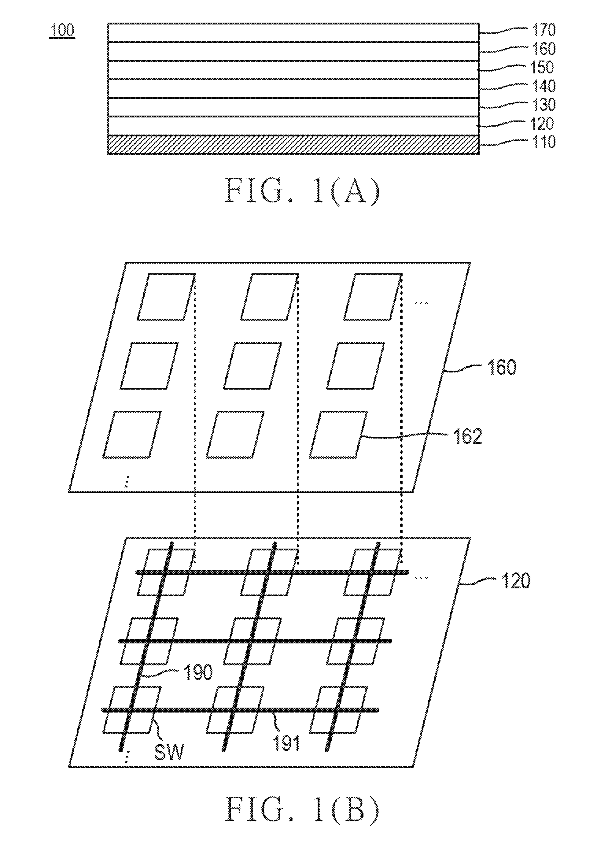
[0049]FIG. 1(A) is a stacked diagram of a biometric feature identification device 100 according to the invention. The biometric feature identification device 100 includes a substrate 110, a switch and trace layer 120, a first insulating layer 130, an electrode shielding layer 140, a second insulating layer 150, an electrode layer 160, and a protection layer 170.

[0050]The substrate 110 is preferably made of glass, polymer film, metal, silicon, or silicide. The electrode layer 160 is arranged at one side of the substrate 110 and has a plurality of electrodes.

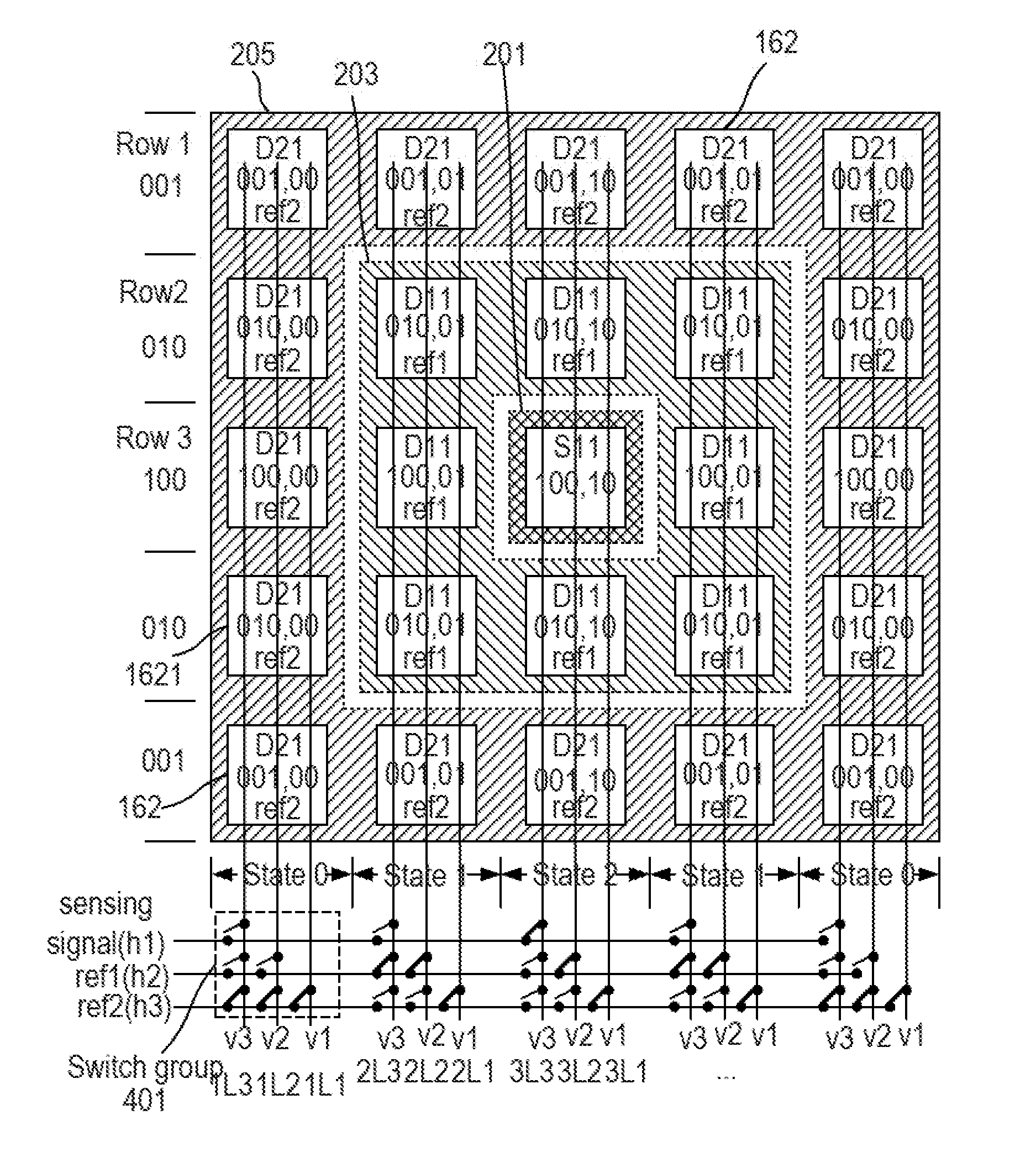
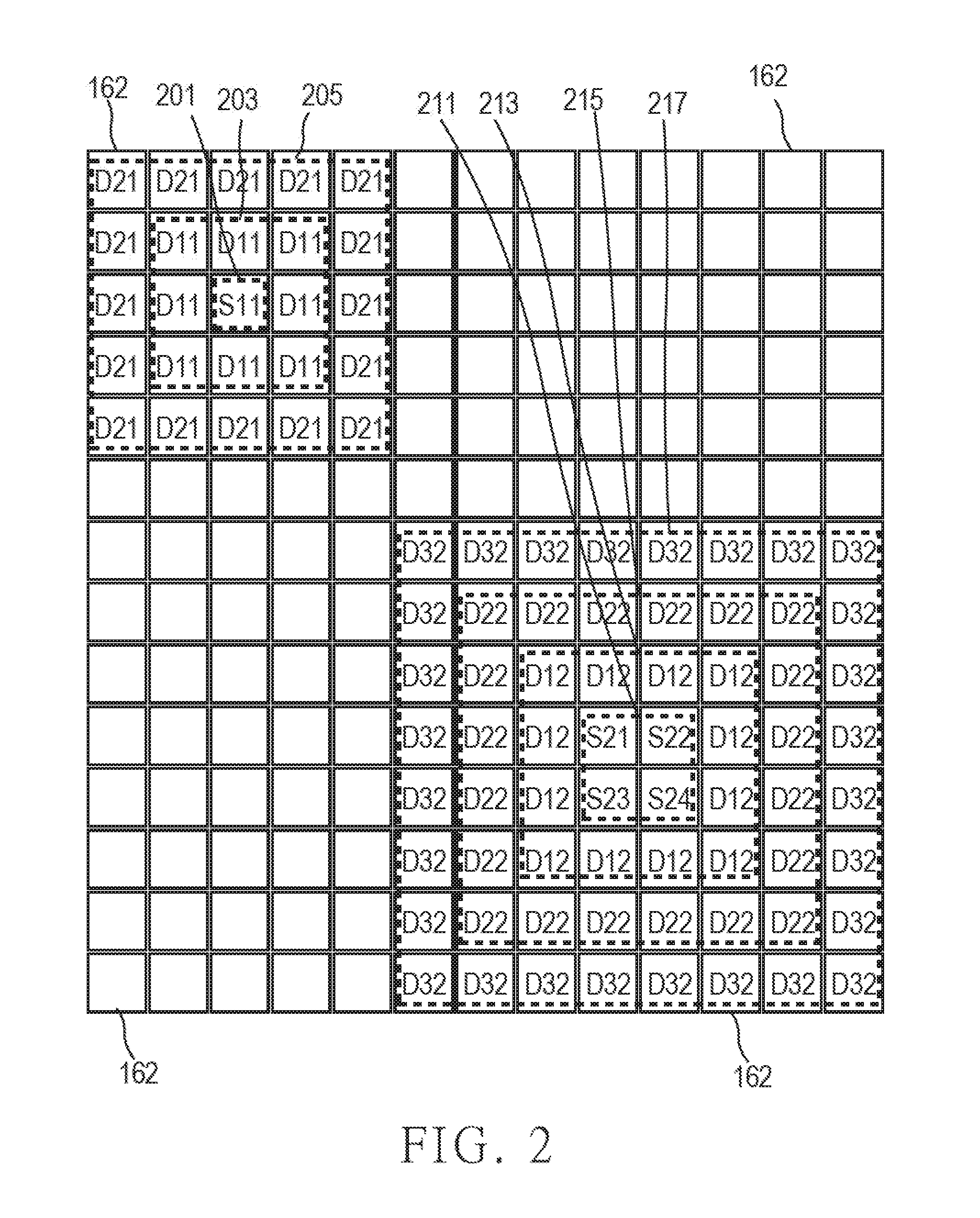
[0051]The switch and trace layer 120 is arranged at one surface of the substrate 110. FIG. 1(B) schematically illustrates the switch and trace layer 120 relative to the electrode layer 160 according to the invention. In FIG. 1(B), the switch and trace layer 120 has a plurality of selection switch groups SW arranged in a matrix form and a plurality of traces 190, 191 arranged in rows and columns. Each longitudinal trace 190 passes ...


PUM


Abstract

A biometric feature identification device includes a substrate, an electrode layer, and a switch and trace layer. The electrode layer is arranged at one side of the substrate and has a plurality of electrodes. The switch and trace layer has a plurality of switches and a plurality of traces. The switches are provided to divide the plurality of electrodes sequentially or dynamically into at least one sensing electrode group and a plurality of deflection electrode groups corresponding thereto. Each sensing electrode group corresponds to at least two deflection electrode groups. Each sensing electrode group has at least one electrode for sensing. Each deflection electrode group has a plurality of electrodes for deflection.

Description

BACKGROUND OF THE INVENTION[0001]1. Field of the Invention[0002]The present invention relates to the technical field of sensing devices and, more particularly, to a biometric feature identification device and method.[0003]2. Description of Related Art[0004]With development of electronic commerce, remote payments have been developed with giant strides, and thus the commercial requirement for biometric feature identification is rapidly expanded. The biometric feature identification technologies can be divided into fingerprint identification, iris identification, DNA identification, and the like. For the efficient, safe, and non-intrusive considerations, the fingerprint identification becomes the first choice. The fingerprint identification technique includes optical, thermal sensing, ultrasonic, and capacitive approaches and, upon considering the device volume, cost, power-saving, reliability and anti-counterfeit, the capacitive approach is the most outstanding one.[0005]Typically, th...

Claims


Application Information

Patent Timeline
Patent Type & Authority Applications(United States)
IPC IPC(8): G06K9/00
CPCG06K9/0002G06V40/1306
Inventor LEE, HSIANG-YUCHIN, SHANGLIN, PING-TSUN
Owner SUPERC TOUCH CORP
Why Eureka
Try Eureka