

Wafer processing method
- Summary
- Abstract
- Description
- Claims
- Application Information
AI Technical Summary
Benefits of technology
Problems solved by technology
Method used
Image

Examples
Embodiment Construction
[0029]A preferred embodiment of the present invention will now be described in detail with reference to the drawings. The present invention is not limited to the preferred embodiment. Further, the components used in the preferred embodiment may include those that can be easily assumed by persons skilled in the art or substantially the elements as those known in the art. Further, the configurations described below may be suitably combined. Further, the configurations may be variously omitted, replaced, or changed without departing from the scope of the present invention.
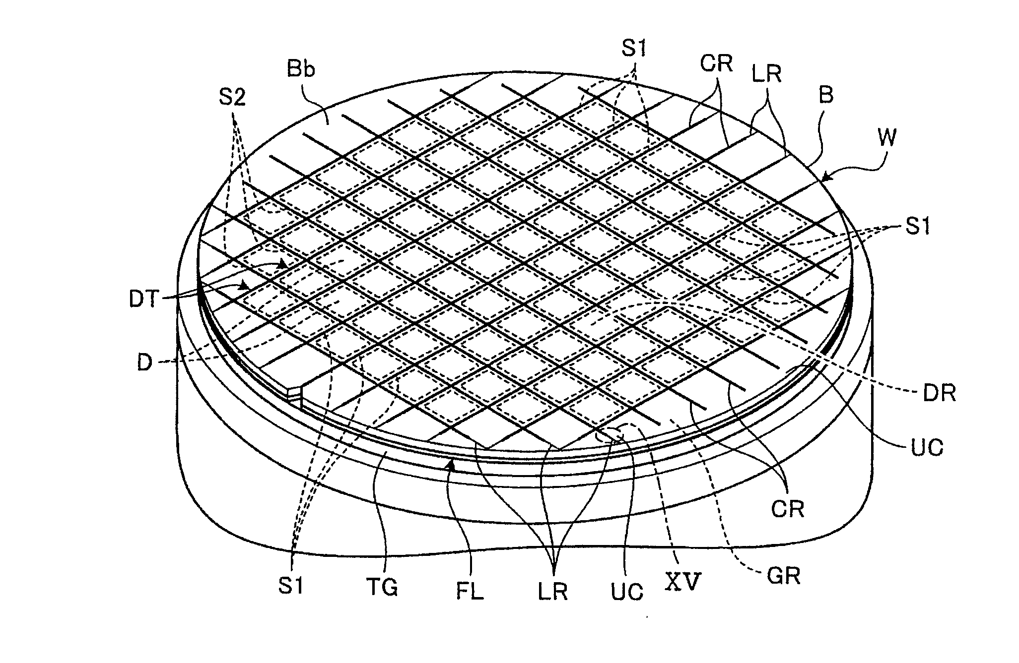
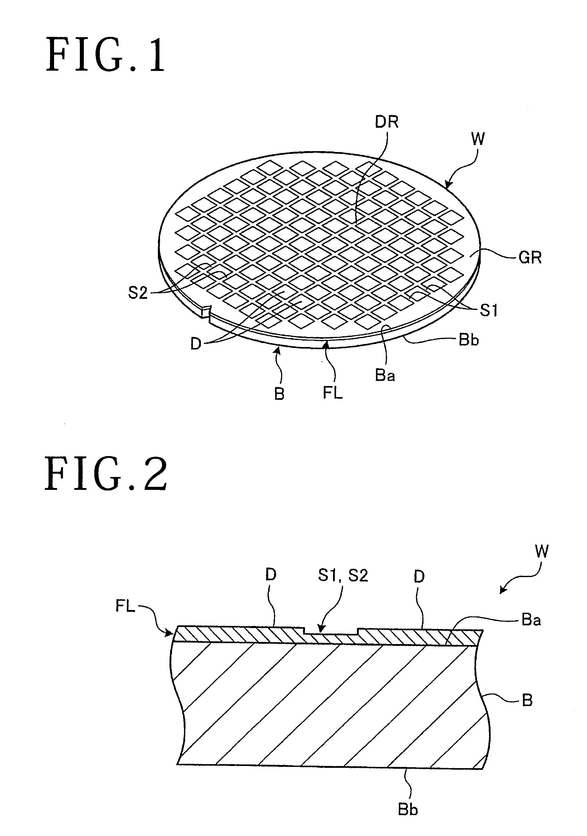
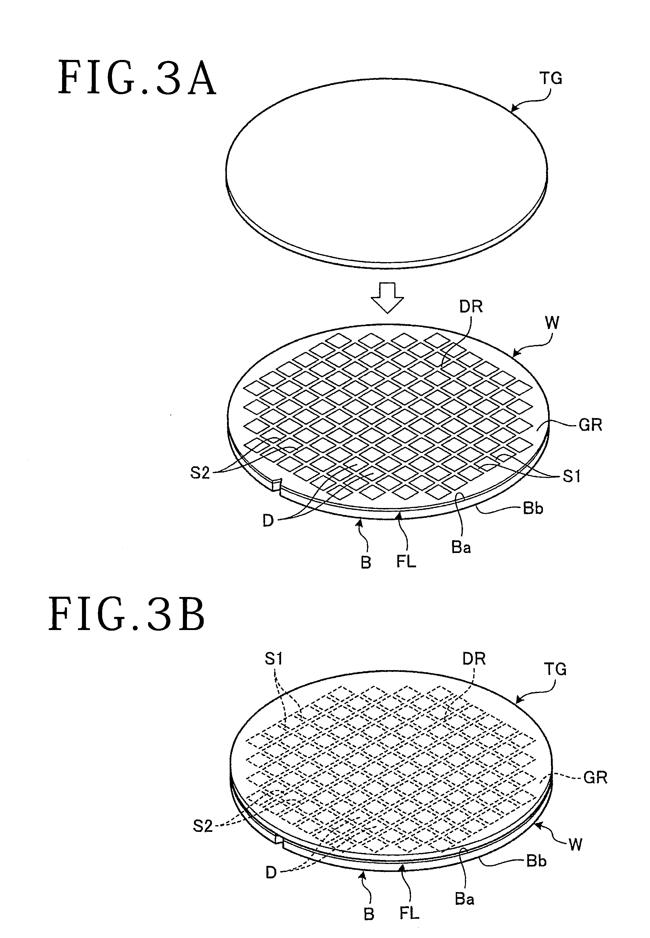
[0030]The wafer processing method (which will be hereinafter referred to simply as processing method) according to the preferred embodiment is a method of processing a wafer W shown in FIGS. 1 and 2. More specifically, the processing method according to the preferred embodiment is a method including the steps of forming a cut groove CR (see FIGS. 8A and 8B) on a back side Bb of a substrate B of the wafer W having a fu...
PUM
| Property | Measurement | Unit |
|---|---|---|
| Area | aaaaa | aaaaa |
| Depth | aaaaa | aaaaa |
Abstract
Description
Claims
Application Information