Zener triggered silicon controlled rectifier with small silicon area

Active Publication Date: 2016-11-24
SEMICON MFG INT (SHANGHAI) CORP
View PDF0 Cites 13 Cited by
  • Summary
  • Abstract
  • Description
  • Claims
  • Application Information

AI Technical Summary

Benefits of technology

[0019]The following description, together with the accompanying drawings, will pro

Problems solved by technology

In the field of semiconductor technology, the electrostatic discharge (ESD) phenomenon poses a major threat to the reliability of an integrated circuit (IC) device.
With the decrease in the feature size of semiconductor technology nodes, the design of ESD protection has become a more difficult and more challenging task in nanoscale CMOS technolo

Method used


Image

  • Zener triggered silicon controlled rectifier with small silicon area
  • Zener triggered silicon controlled rectifier with small silicon area
  • Zener triggered silicon controlled rectifier with small silicon area

Examples


Example

First Embodiment

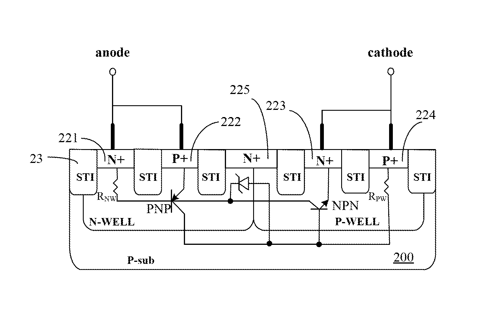
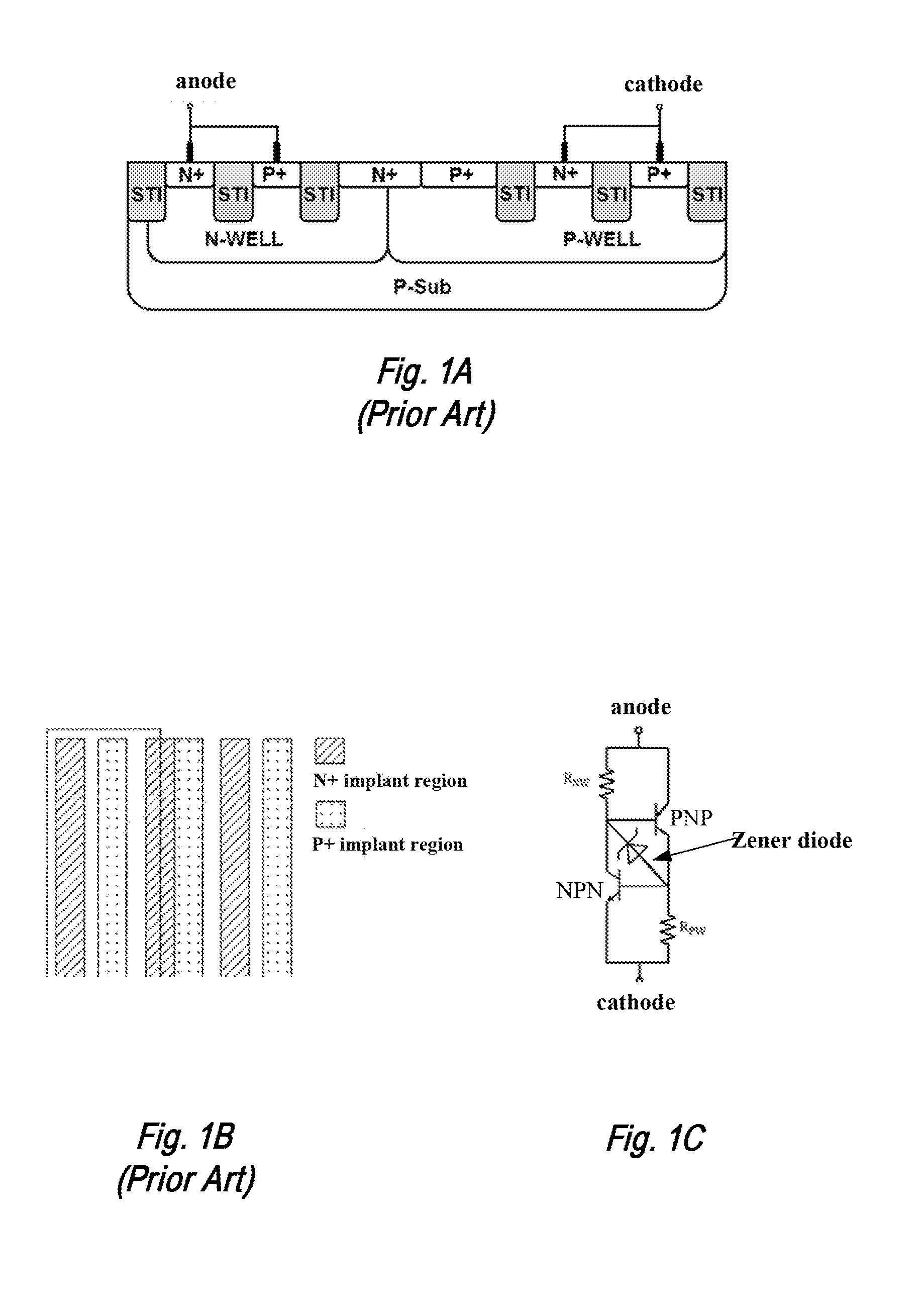
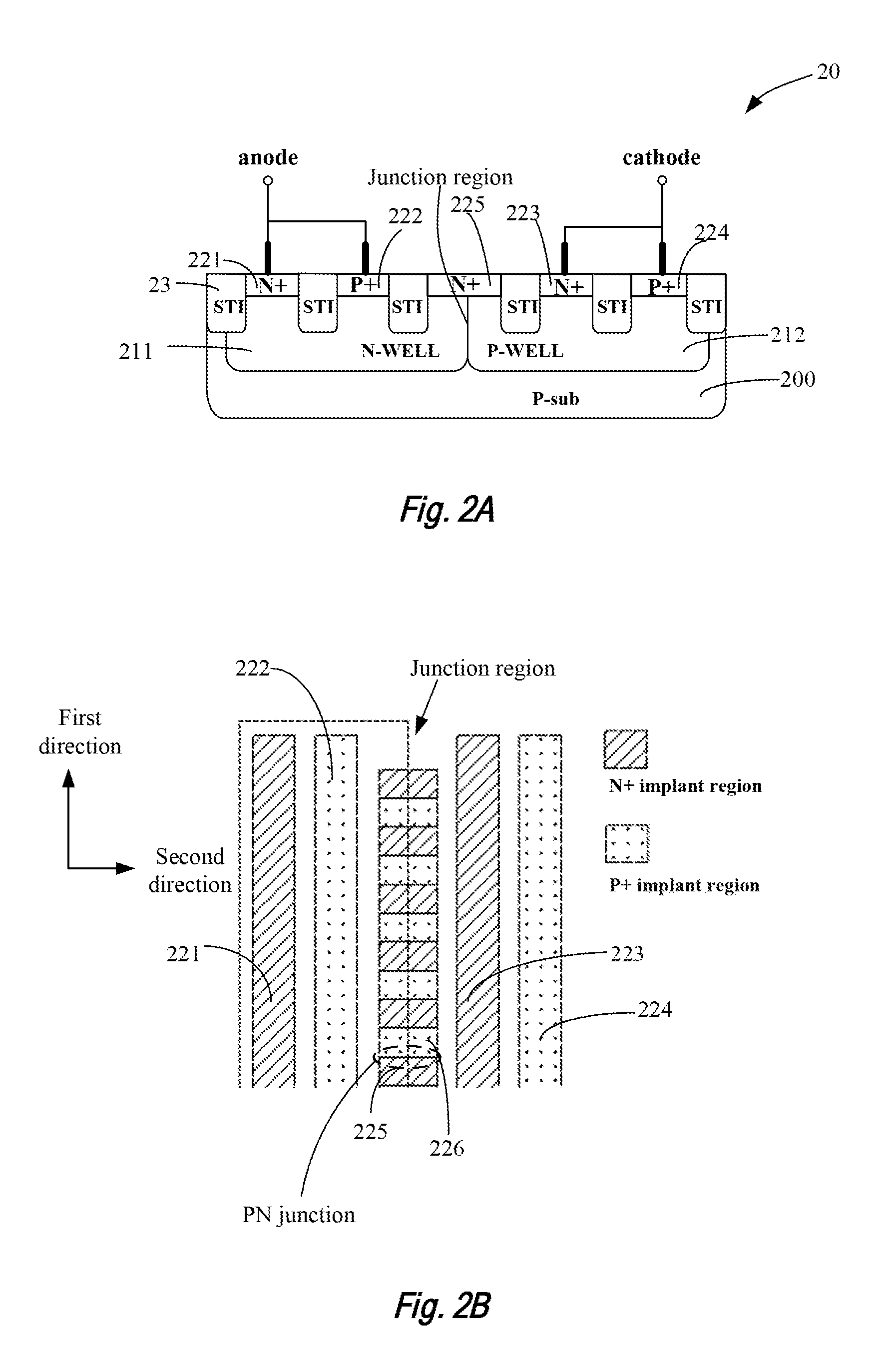
[0034]FIG. 2A is a cross-sectional view of a semiconductor device 20 according to an embodiment of the present invention. FIG. 2B is a top plane view of the semiconductor device of FIG. 2A. Referring to FIG. 2A and 2B, a semiconductor device according to the present invention includes a semiconductor substrate 200. Semiconductor substrate 200 may be one of silicon, silicon on insulator (SOI), stacked silicon on insulator (SSOI), stacked SiGe on insulator (S—SiGeOI), SiGe on insulator (SiGeOI), Ge on insulator (GeOI), and the like. Semiconductor substrate 200 may be a P-type semiconductor substrate doped with a P-type dopant.

[0035]Semiconductor substrate 200 further includes a N-well 211 and a P-well 212 that are disposed adjacent to each other and extending along a first direction within the P-type semiconductor substrate 200. N-well 211 includes a first N+ implanted (doped) region 221 and a first P+ implanted region 222, both of which are extending along the first d...

Example

Second Embodiment

[0044]Embodiments of the present invention also provide an electronic device including an electronic component and a semiconductor device connected to the electronic component. The semiconductor device can be the semiconductor device of embodiment 1.

[0045]Because the semiconductor device consumes a small surface area of the semiconductor substrate while providing a faster turn-on time of the SCR device, the electronic device incorporated such semiconductor device will have improved ESD protection.

[0046]In accordance with the present invention, the electronic device may be a mobile phone, a laptop computer, a netbook, a tablet PC, a game console, a TV, a DVD player, a GPS device, a camera, a voice recorder, MP3, MP4, PSP players, and other semiconductor devices including intermediate products and electronic components that incorporate the above-described semiconductor device with improved ESD protection.

[0047]While the present invention is described herein with refer...


PUM


Abstract

A semiconductor device includes a P-type semiconductor substrate, an N-well and a P-well disposed adjacent to each other and extending along a first direction within the P-type semiconductor substrate, a first N+ doped region and a first P+ doped region extending along the first direction within the N-well and spaced away from each other along a second direction perpendicular to the first direction, a second N+ doped region and a second P+ doped region extending along the first direction within the P-well and spaced away from each other along the second direction, and a plurality of third N+ doped regions and a plurality of P+ doped regions alternatively disposed in a junction region formed between the N-well and P-well the third N+ doped regions. The third N+ doped regions and the third P+ doped regions form a Zener diode.

Description

CROSS-REFERENCES TO RELATED APPLICATIONS[0001]This application claims priority to Chinese patent application No. 201510255838.X, filed May 19, 2015, the content of which is incorporated herein by reference in its entirety.[0002]This application is related to co-pending application entitled “An Improved Low Voltage Triggered Silicon Controlled Rectifier with High Holding Voltage and Small Silicon Area,” by Lei Zhong, Hongwei Li, Wei Li, Guang Chen, and Huijuan Cheng, filed ______ (U.S. application Ser. No. ______), the content of which is incorporated by reference in its entirety.FIELD OF INVENTION[0003]The present invention relates to semiconductor technology, and more particularly to a Zener triggered silicon controlled rectifier and an electronic apparatus containing the same.BACKGROUND OF THE INVENTION[0004]In the field of semiconductor technology, the electrostatic discharge (ESD) phenomenon poses a major threat to the reliability of an integrated circuit (IC) device. With the d...

Claims


Application Information

Patent Timeline
IPC IPC(8): H01L27/02H01L29/866H01L27/06
CPCH01L27/0262H01L29/866H01L27/0647H01L29/87H01L29/0649H01L27/0783
Inventor ZHONG, LEILI, HONGWEILEI, WEICHENG, HUIJUAN
Owner SEMICON MFG INT (SHANGHAI) CORP
Why Eureka
Try Eureka