Organic Light Emitting Device

a light-emitting device and organic technology, applied in the direction of organic semiconductor devices, solid-state devices, semiconductor devices, etc., can solve the problems of reducing affecting the color change rate, and affecting the efficiency so as to improve the efficiency and a lifetime of the organic light-emitting device, and smoothly transfer electron

Active Publication Date: 2016-11-24
LG DISPLAY CO LTD
View PDF1 Cites 14 Cited by
  • Summary
  • Abstract
  • Description
  • Claims
  • Application Information

AI Technical Summary

Benefits of technology

[0022]According to an aspect of the present disclosure, there is provided an organic light emitting device. The organic light emitting device includes a first electrode and a second electrode disposed to face each other. The organic light emitting device further includes a plurality of light emitting units laminated between the first electrode and the second electrode and each including an organic emitting layer and a charge generation layer between the light emitting units. The charge generation layer includes an N-type charge generation layer disposed to be in direct contact with at least a first organic emitting layer of the light emitting units. Herein, a highest occupied molecular orbital (HOMO) level of the N-type charge generation layer is higher than a HOMO level of the first organic emitting layer in contact with the N-type charge generation layer. In the organic light emitting device according to an exemplary embodiment of the present disclosure, the N-type charge generation layer and the first organic emitting layer are disposed to be in direct contact with each other. Further, HOMO levels of the N-type charge generation layer and the organic emitting layer are appropriately regulated. Thus, it is possible to improve a color change rate based on a viewing angle and also possible to improve efficiency and a lifetime of the organic light emitting device.
[0023]According to another aspect of the present disclosure, there is provided an organic light emitting device. The organic light emitting device includes a first electrode and a second electrode disposed to face each other. The organic light emitting device further includes a first light emitting unit disposed on the first electrode and including a first organic emitting layer, a second light emitting unit including a second organic emitting layer, and a third light emitting unit including a third organic emitting layer. A first charge generation layer disposed between the first light emitting unit and the second light emitting unit includes a first N-type charge generation layer. A second charge generation layer disposed between the second light emitting unit and the third light emitting unit includes a second N-type charge generation layer. Herein, the first N-type charge generation layer is disposed to be in direct contact with the first organic emitting layer to smoothly transfer electrons from the first N-type charge generation layer to the first organic emitting layer, or the second N-type charge generation layer is disposed to be in direct contact with the second organic emitting layer to smoothly transfer electrons from the second N-type charge generation layer to the second organic emitting layer. In the organic light emitting device according to another exemplary embodiment of the present disclosure, at least one bonding surface between the N-type charge generation layer and the organic emitting layer is formed in the structure including the three light emitting units. Thus, it is possible to achieve an improved color change rate based on a viewing angle in a structure including a plurality of light emitting units.

Problems solved by technology

If a plurality of light emitting units is laminated as in the OLED device having a tandem structure, it is difficult for holes and electrons generated from an anode and a cathode to be smoothly transferred to each of the plurality of organic light emitting layers.
Thus, efficiency of the organic light emitting device may be reduced.
Therefore, numerous manufacturing processes are required.
Therefore, optical characteristics related to a color change rate based on a viewing angle may deteriorate.
However, if the ETL does not have a high mobility in the organic light emitting device including the multi-layer light emitting unit, electrons cannot be smoothly transferred from the N-type charge generation layer to the organic EML at a low current density, i.e., from about 0.01 mA / cm2 to about 1 mA / cm2.
Thus, the organic emitting layer cannot readily emit light and excitons are undesirably generated from another layer such as a charge generation layer.
Therefore, the overall device performance, such as device efficiency and a lifetime, of the organic light emitting device is considerably reduced.
Such increase in resistance occurs when the organic light emitting device is driven at a low current density and electrons cannot be smoothly transferred from an N-type charge generation layer to an organic emitting layer.

Method used


Image

  • Organic Light Emitting Device
  • Organic Light Emitting Device
  • Organic Light Emitting Device

Examples


Embodiment Construction

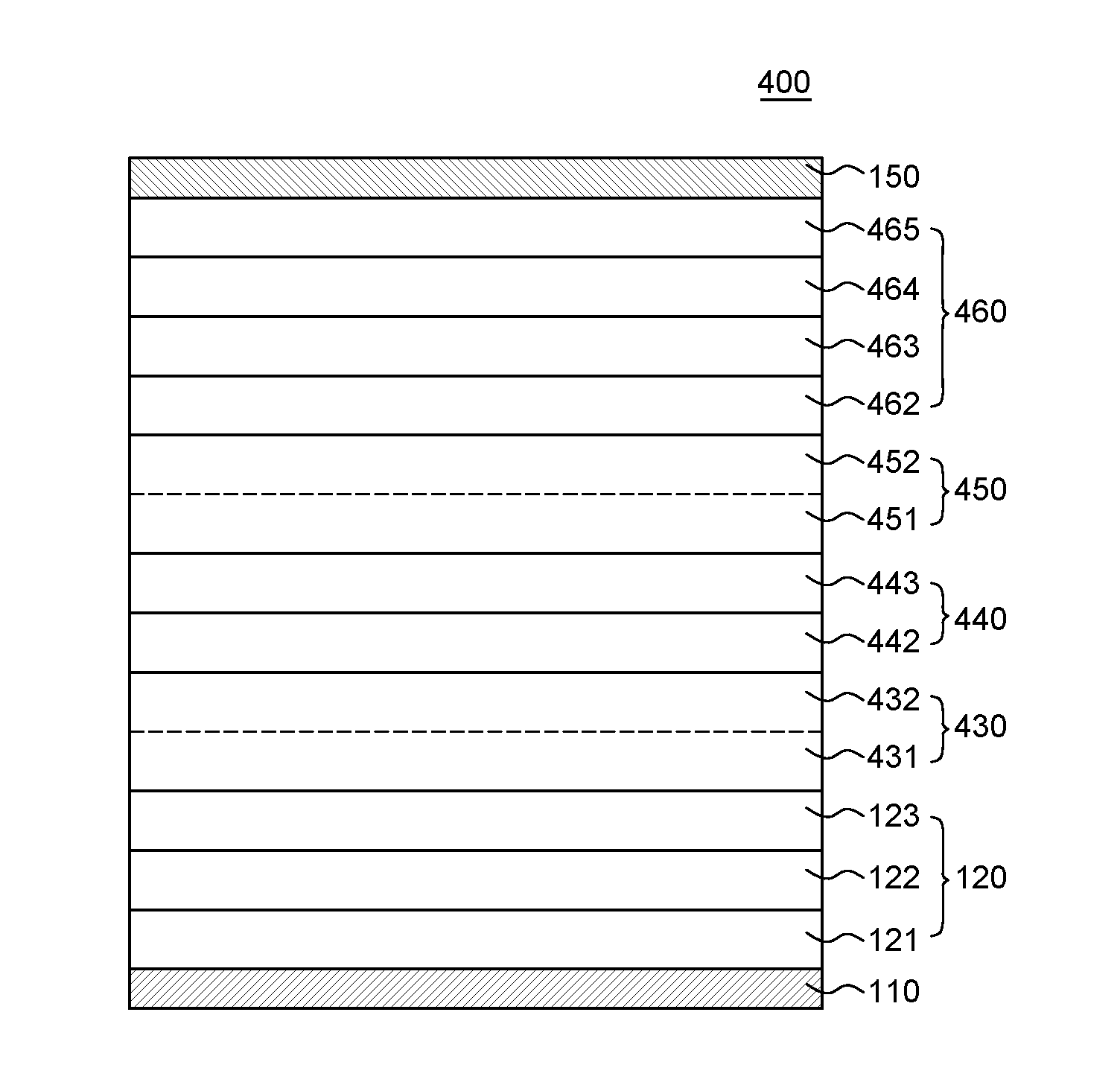
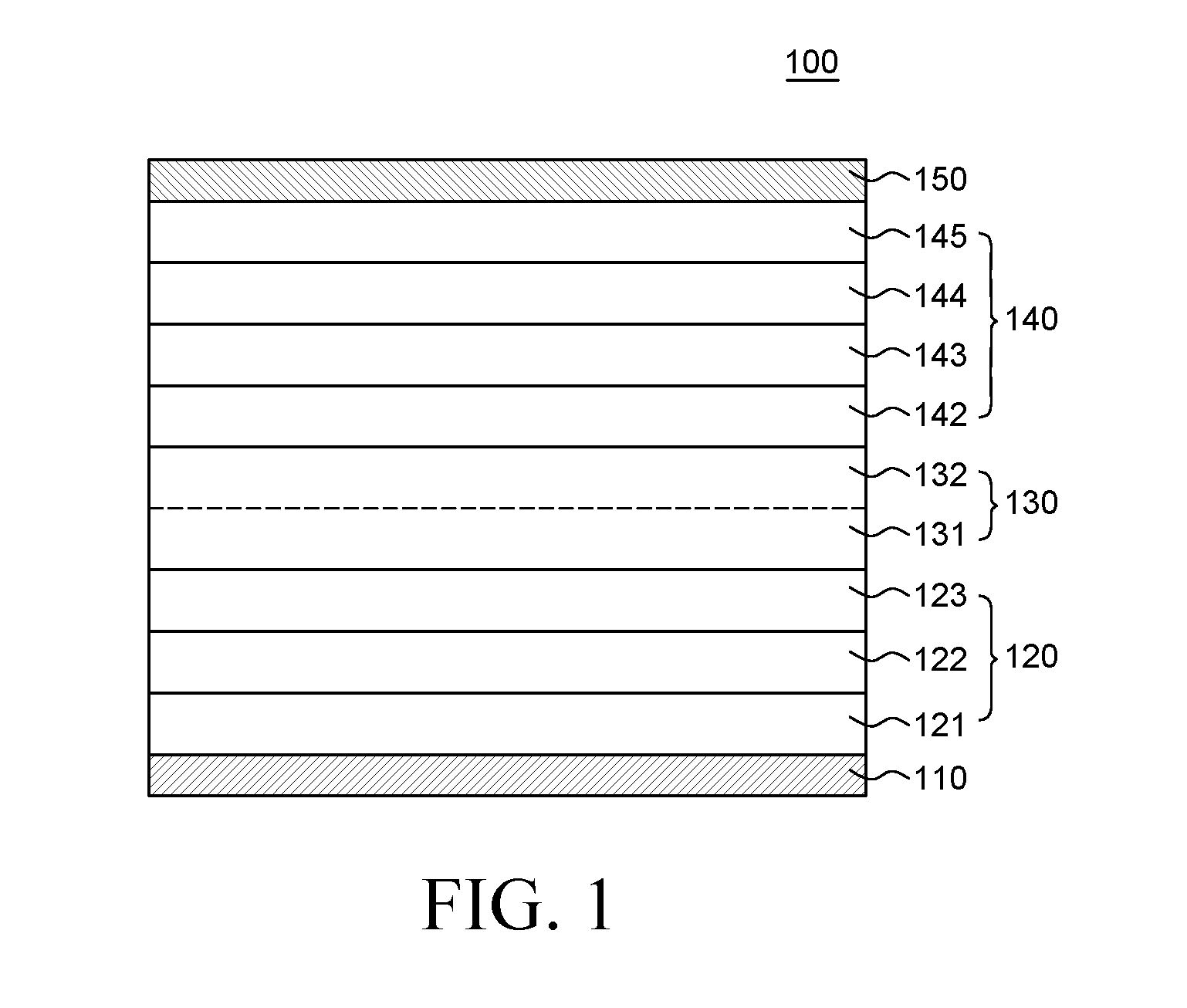
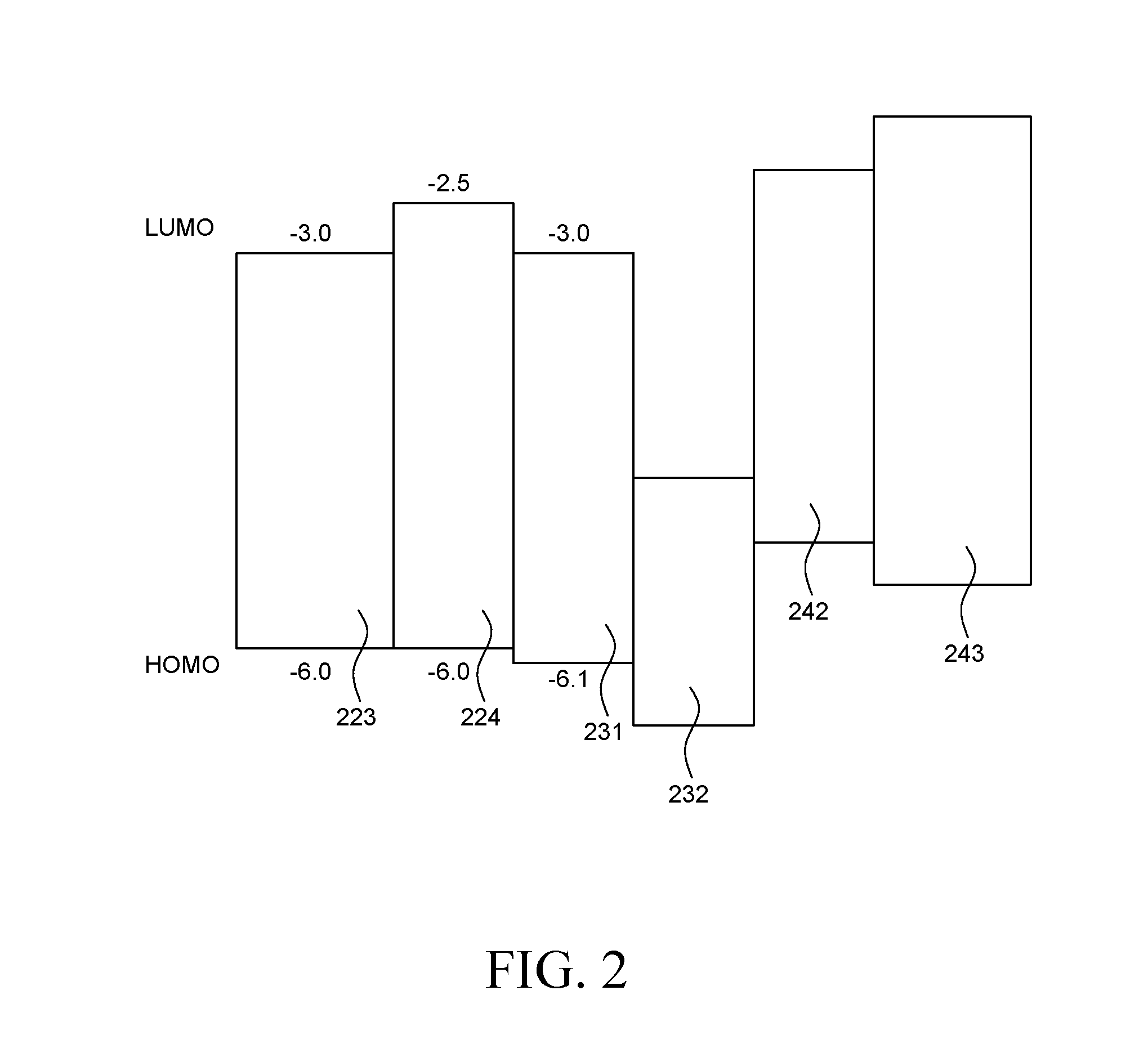
[0034]Advantages and features of the present disclosure, and methods for accomplishing the same will be more clearly understood from exemplary embodiments described below with reference to the accompanying drawings. However, the present disclosure is not limited to the following exemplary embodiments but may be implemented in various different forms. The exemplary embodiments are provided only to complete disclosure of the present disclosure and to fully provide a person having ordinary skill in the art to which the present disclosure pertains with the category of the disclosure, and the present disclosure will be defined by the appended claims.

[0035]The shapes, sizes, ratios, angles, numbers, and the like illustrated in the accompanying drawings for describing the exemplary embodiments of the present disclosure are merely examples, and the present disclosure is not limited thereto. Like reference numerals generally denote like elements throughout the present specification. Further,...


PUM


Abstract

Provided is an organic light emitting device. The organic light emitting device includes a plurality of light emitting units laminated between a first electrode and a second electrode and each including an organic emitting layer, and a charge generation layer between the light emitting units. Further, the charge generation layer includes an N-type charge generation layer disposed to be in direct contact with an organic emitting layer of the adjacent light emitting unit and HOMO levels of the N-type charge generation layer and the organic emitting layer are regulated. Thus, a color change rate based on a viewing angle can be improved, and efficiency and a lifetime of the organic light emitting device can be improved.

Description

CROSS-REFERENCE TO RELATED APPLICATIONS[0001]This application claims the priority of Republic of Korea Patent Application No. 10-2015-0072267 filed on May 23, 2015, in the Korean Intellectual Property Office, the disclosure of which is incorporated herein by reference.BACKGROUND[0002]1. Field[0003]The present disclosure relates to an organic light emitting device and more particularly, to an organic light emitting device having a multi-layer light emitting structure and capable of improving a color change rate based on viewing angle, efficiency, and a lifetime of the device.[0004]2. Description of the Related Art[0005]An organic light emitting display (OLED) device is a self-light emitting display device and does not need a separate light source as in a liquid crystal display device. Thus, the OLED device can be manufactured into a lightweight and thin form. Further, the OLED device is advantageous in terms of power consumption since it is driven with a low voltage. Also, the OLED d...

Claims


Application Information

Patent Timeline
Patent Type & Authority Applications(United States)
IPC IPC(8): H01L27/32H01L51/52H01L51/50
CPCH01L27/322H01L51/5088H01L51/5056H01L51/5072H01L51/5271H01L51/5004H01L51/0059H01L2251/552H01L51/0072H01L51/005H01L51/006H01L51/0058H01L51/5278H10K85/6572H10K50/11H10K2101/40H10K50/19H10K2101/30H10K59/38H10K50/15H10K50/16H10K50/17H10K50/856H10K85/60H10K85/626H10K85/631H10K85/633
Inventor HEO, JEONGHAENGSONG, JAEILLEE, SANGGUNAHN, SOYEON
Owner LG DISPLAY CO LTD
Why Eureka
Try Eureka