Liquid crystal display device

a liquid crystal display and display device technology, applied in the field of liquid crystal display devices, can solve the problems of inability to completely transmit light through the black matrixes, affecting the flatness of the color filter, and difficult to stably manufacture black matrixes with a thin line having a width of 4 m, etc., to achieve the effect of improving visibility, increasing aperture ratio, and improving transmittan

Active Publication Date: 2016-12-15
TOPPAN PRINTING CO LTD
View PDF11 Cites 30 Cited by
  • Summary
  • Abstract
  • Description
  • Claims
  • Application Information

AI Technical Summary

Benefits of technology

[0060]One aspect of the present invention can increase an aperture ratio to thereby provide a liquid crystal display device that has improved transmittance and improved visibility, for example. Moreover, according to one aspect of the present invention, it is possible to provide a liquid crystal display device equipped with a black electrode that has high performance in detecting a position of the pointer such as a finger, and has a small resistance value and low reflectance, for example.
[0061]Moreover, in one aspect of the present invention, the light absorptive resin layer patterns are provided between the first transparent substrate and the metal layer patterns. Accordingly, when the liquid crystal panel performs black display, it is possible to match a hue or a reflection color to the black color of a bezel (a black frame on the perimeter of the display unit) by a plurality of metal wirings (a source line, a gate line) or the like formed in the second transparent substrate in the array substrate, for example, and improve visibility. Furthermore, it is possible to provide a liquid crystal display device that has high aperture ratio and additionally has a touch sensing function. Furthermore, it is possible to utilize a high black display, which is a feature of vertically-aligned liquid crystals.
[0062]In addition, one aspect of the present invention proposes a touch electrode flexibly adaptable up to a pixel size that is ensured to achieve high definition, and capable of improving noise tolerance. This touch electrode, in contrast to an externally-added touch panel, can support stylus input.

Problems solved by technology

It has been revealed that a smaller thickness of black matrixes adversely affects the flatness of the color filters.
For example, since black matrixes have high light shielding properties, it is difficult to stably manufacture a pattern of black matrixes with a thin line having a width of 4 μm or smaller, by photolithography.
Materials with high light properties used for black matrixes suffer from a difficulty of not being able to completely transmit light therethrough in the thickness direction at light exposure.
Moreover, from the viewpoint of alignment, it is very difficult to form a black matrix with a thin line width of 4 μm or less through two-step photolithography, i.e. to form it with two layers, for the purpose of improving light shielding properties.
Forming a black matrix through two-step photolithography tends to cause variation of line width or display unevenness, due to alignment errors.
Therefore, it has been difficult to form a black matrix by two-step photolithography processes.

Method used


Image

  • Liquid crystal display device
  • Liquid crystal display device
  • Liquid crystal display device

Examples


first embodiment

[0084]With reference to FIGS. 1 to 13, a first embodiment of a liquid crystal display device according to the present invention will be described. The scale ratio of thicknesses or dimension of components is varied between the drawings as appropriate for the sake of clarity.

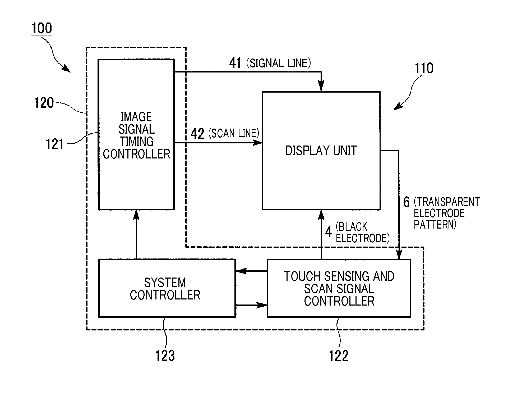
[0085]As shown in FIG. 1, a liquid crystal display device 100 of the present embodiment includes a display unit 110, and a control unit 120 for controlling the display unit 110 and a touch sensing function.

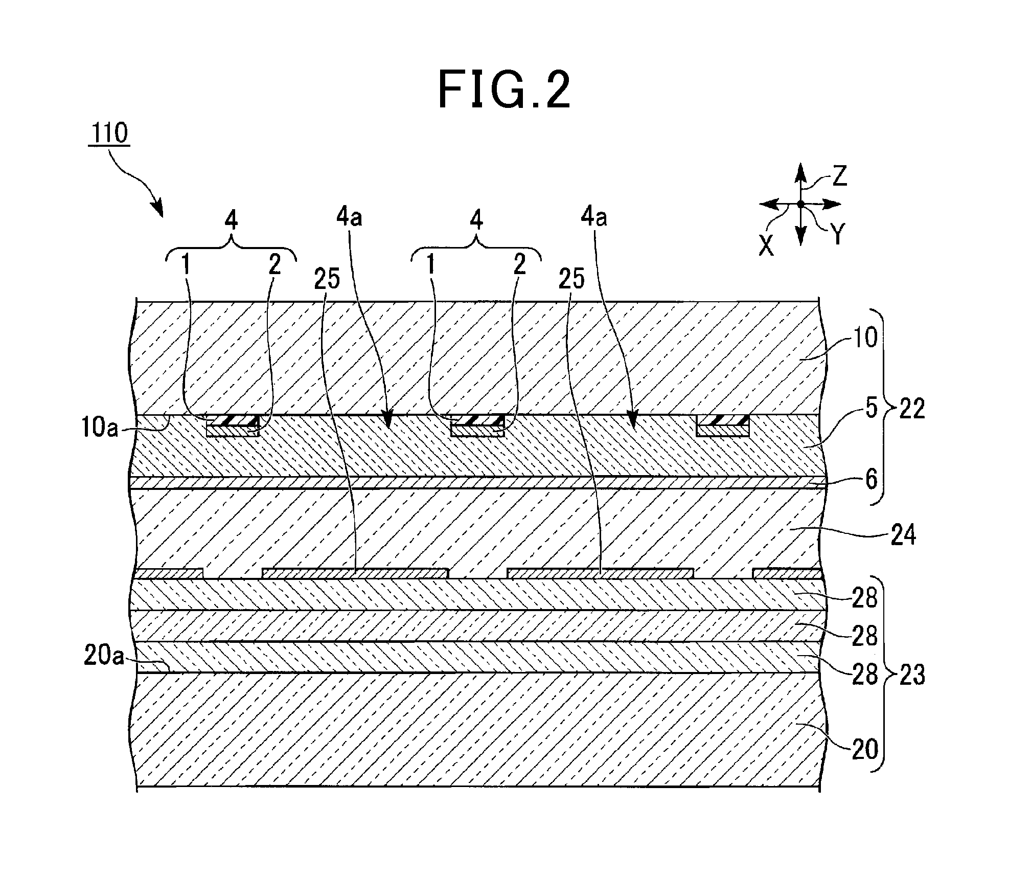
[0086]As shown in FIG. 2, the display unit 110 has a configuration in which a liquid crystal display device substrate 22 (display substrate), a liquid crystal layer 24, and an array substrate 23 are laminated in this order. The display unit 110 performs a display operation in a normally-black mode. Specifically, the display unit 110 is configured by bonding a first transparent substrate 10 of the liquid crystal display device substrate 22, which will be described below, and a second transparent substrate 20 of ...

second embodiment

[0206]Referring now to FIGS. 14 to 17, a second embodiment of the present invention will be described. Those components which are identical with those of the foregoing embodiment are given the same reference signs to omit duplicate description and to provide description focusing on differences.

[0207]As shown in FIG. 14, a display unit 111 of the present embodiment includes a liquid crystal display device substrate 22A, in place of the liquid crystal display device substrate 22 of the display unit 110 of the first embodiment. The liquid crystal display device substrate 22A is configured such that the pixel opening 4a of each black electrode 4 of the liquid crystal display device substrate 22 is provided with any of a red pixel R formed of a red layer, a green pixel G formed of a green layer, and a blue pixel B formed of a blue layer. The red pixel R, green pixel G, and blue pixel B are each inserted between the metal layer pattern 2 and the transparent resin layer 5 in the laminating...

third embodiment

[0217]The following description addresses a third embodiment of the present invention. Those components which are identical with those of the foregoing embodiments are given the same reference signs to omit duplicate description and to provide description focusing on differences.

[0218]The present embodiment is similar to the first embodiment except for the configuration of the metal layer patterns 2, i.e., the configuration of the black electrodes 4. Therefore, FIG. 2 is incorporated by reference. However, duplicate description is omitted, and the metal layer pattern 2 having differences will be described. The black electrodes 4 of the present embodiment can be used as the black electrodes of the second embodiment described above and a fourth embodiment which will be described below.

[0219]In the present embodiment, the metal layer patterns 2 shown in FIG. 2 are each formed of a layer having a total thickness of 0.21 μm. This layer is obtained by laminating two layers, namely, a firs...


PUM

PropertyMeasurementUnit
thicknessaaaaaaaaaa
optical densityaaaaaaaaaa

Abstract

A liquid crystal display device with a surface of a first transparent substrate, the surface of the substrate facing a liquid crystal layer, a plurality of light absorptive resin layer patterns, a plurality of metal layer patterns, a transparent resin layer, and a plurality of transparent electrode patterns are laminated in this order; the plurality of light absorptive resin layer patterns and the plurality of metal layer patterns have openings formed therein and formed into the same shape when viewed in a laminating direction; the plurality of metal layer patterns are arrayed in a first direction, being insulated from each other; the plurality of transparent electrode patterns are arrayed in a second direction perpendicular to the first direction, being insulated from each other; each metal layer pattern has at least one of an alloy layer mainly containing copper, and a copper layer.

Description

CROSS-REFERENCE TO RELATED PATENT APPLICATIONS[0001]This application is a continuation application filed under 35 U.S.C. §111(a) claiming the benefit under 35 U.S.C. §§120 and 365(c) of International Application No. PCT / JP2014 / 081174 filed on Nov. 26, 2014, which is based upon and claims the benefit of priority of Japanese Patent Application No. 2014-038821, filed on Feb. 28, 2014, the entire contents of them all are hereby incorporated by reference.TECHNICAL FIELD[0002]The present invention relates to a liquid crystal display device having a liquid crystal panel incorporating a touch sensing function, and having a high aperture ratio and good visibility. The present invention can provide a liquid crystal display device equipped with a touch sensing electrode that uses a low-resistance metal layer pattern favorable for an electrode for use in touch sensing, and has high light shielding properties of transmission light, the metal layer pattern exhibiting substantially black reflected...

Claims


Application Information

Patent Timeline
Patent Type & Authority Applications(United States)
IPC IPC(8): G06F3/041G02F1/1343G02F1/1337G02F1/1368G02F1/1333G06F3/044G02F1/1362
CPCG02F1/134309G06F3/0412G02F1/136286G02F1/1368G02F1/133345G02F1/1337G02F1/13338G02F1/137G02F2001/13712G02F2001/133742G02F2001/136295G02F2201/52G02F2001/133302G02F1/133514G02F1/133512G02F1/133528G02F2201/121G02F2201/123G06F3/0418G06F3/044G02F1/13439G02F1/13306G06F2203/04103G06F3/0445G06F3/04182G09G3/36G02F1/13712G02F1/133302G02F1/133742G02F1/136295
Inventor KIMURA, YUKIHIROFUKUYOSHI, KENZO
Owner TOPPAN PRINTING CO LTD
Why Eureka
Try Eureka