

Inspection apparatus and inspection method
a technology of inspection apparatus and inspection method, which is applied in the direction of material analysis by optical means, instruments, photomechanical treatment originals, etc., can solve the problems of reducing the light quantity of the light transmitted through the polarized beam splitter, and affecting the accuracy of inspection results, so as to achieve accurate cd map, accurate line width error, and easy and accurate detection of defects
- Summary
- Abstract
- Description
- Claims
- Application Information
AI Technical Summary
Benefits of technology
Problems solved by technology
Method used
Image

Examples
first embodiment
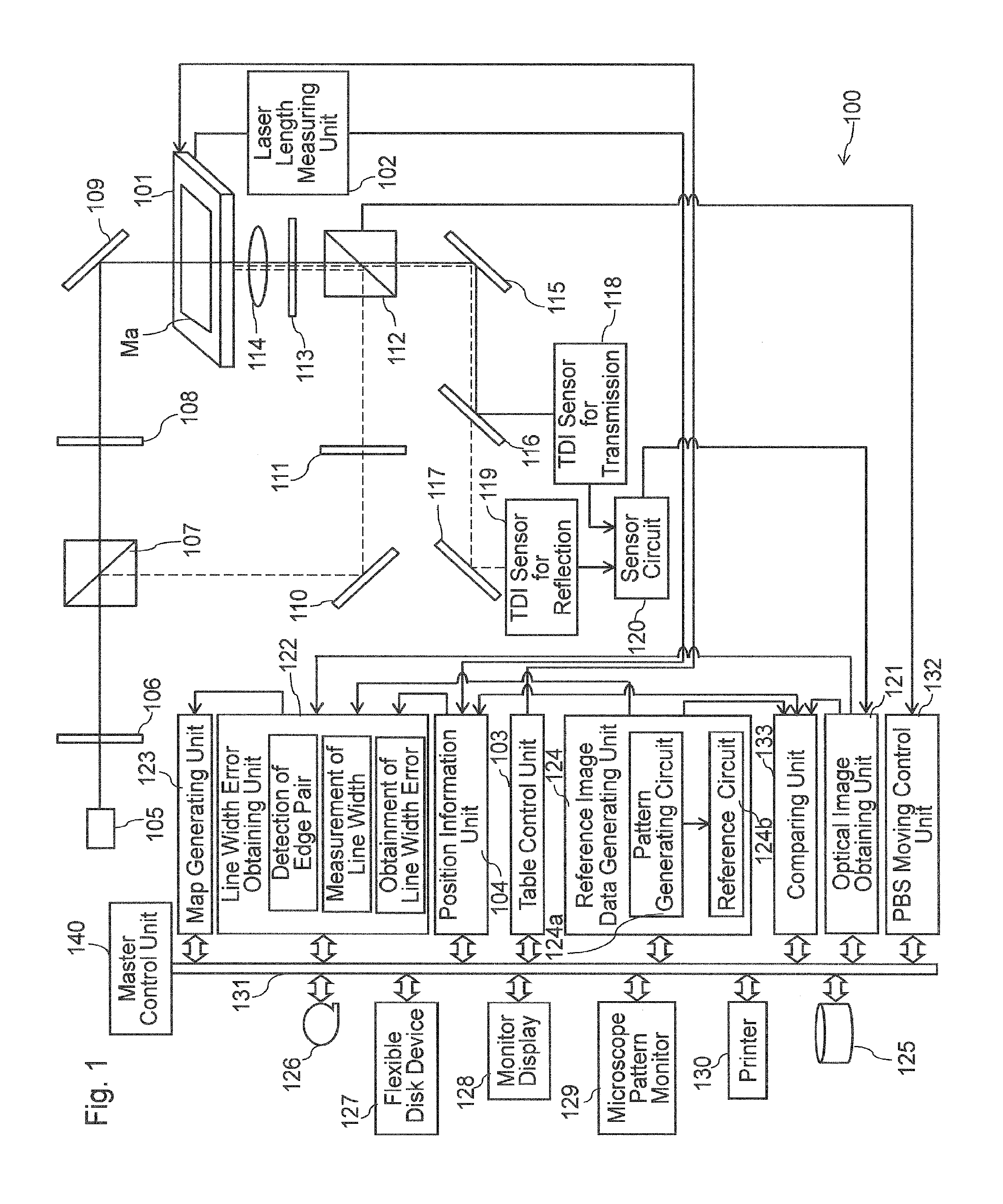
[0027]FIG. 1 is a schematic configuration diagram of the inspection apparatus 100 according to the present embodiment. The inspection apparatus 100 detects a defect in the inspection object by obtaining optical image data of the inspection object, and then compares the optical image data corresponding to reference image data. Further, the inspection apparatus 100 obtains a line width error (ΔCD) of the inspection object, and then generates a line width error map (ΔCD map) from the line width error. The fundamental construction of the inspection apparatus 100 will be described as follows.
[0028]The components of the inspection apparatus 100, for obtaining optical data of the mask Ma, as one example of the object to be inspected, includes a table 101 that is movable in a horizontal direction (X-direction and / or Y-direction) and a rotational direction (θ-direction), a laser length measuring unit 102 as a position measuring unit that measures position coordinates of the table 101, a ligh...
second embodiment
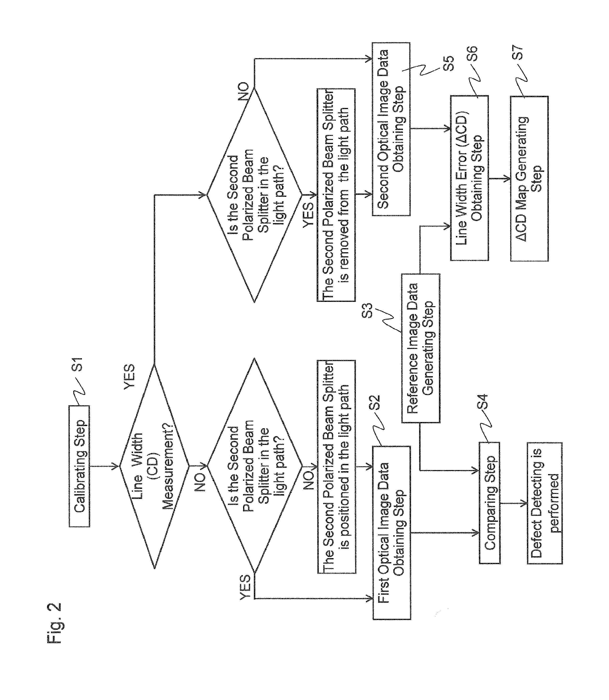
[0118]FIG. 11 is a flowchart of the inspection method according to the present embodiment. As shown in FIG. 11, the inspection method according to the present embodiment includes a calibrating step S11, a first optical image data obtaining step S12, a reference image data generating step S13, a comparing step S14, a first line width error obtaining step S15, a second optical image data obtaining step S16, a second line width error obtaining step S17, a line width error correcting step S18, and a ΔCD map generating step S19. The comparing step S14 is one example of the defect detecting step according to the present invention.
[0119]The inspection method according to the present embodiment can also be performed using the inspection apparatus 100 as shown in FIG. 1 and described in the first embodiment. The inspection method according to the present embodiment will be described as follows referring to FIG. 1, FIG. 11, etc.
11)>
[0120]The explanation of the calibrating step S11 shown in FI...
PUM
| Property | Measurement | Unit |
|---|---|---|
| length | aaaaa | aaaaa |
| width | aaaaa | aaaaa |
| threshold | aaaaa | aaaaa |
Abstract
Description
Claims
Application Information