Method for manufacturing polycrystalline gate structure

A polysilicon gate and polysilicon layer technology, which is applied in semiconductor/solid-state device manufacturing, electrical components, semiconductor devices, etc., can solve problems such as short channels, channel narrowing, polysilicon line disconnection, etc., to reduce manufacturing costs and improve The effect of the overall electrical performance

Active Publication Date: 2014-03-19
SEMICON MFG INT (SHANGHAI) CORP +1
View PDF2 Cites 0 Cited by
  • Summary
  • Abstract
  • Description
  • Claims
  • Application Information

AI Technical Summary

Problems solved by technology

Specifically, as Figure 1D As shown in , the polysilicon line in the polysilicon gate structure in the second region 100N obviously "necked" (necking) , resulting in narrowing of the channel, thereby causing the short channel effect
In addition, severe "necking" may also cause disconnection of polysilicon lines

Method used


Image

  • Method for manufacturing polycrystalline gate structure
  • Method for manufacturing polycrystalline gate structure
  • Method for manufacturing polycrystalline gate structure

Examples


Embodiment Construction

[0039] In the following description, a lot of specific details are given in order to provide a more thorough understanding of the present invention. However, it is obvious to those skilled in the art that the present invention can be implemented without one or more of these details. In other examples, in order to avoid confusion with the present invention, some technical features known in the art are not described.

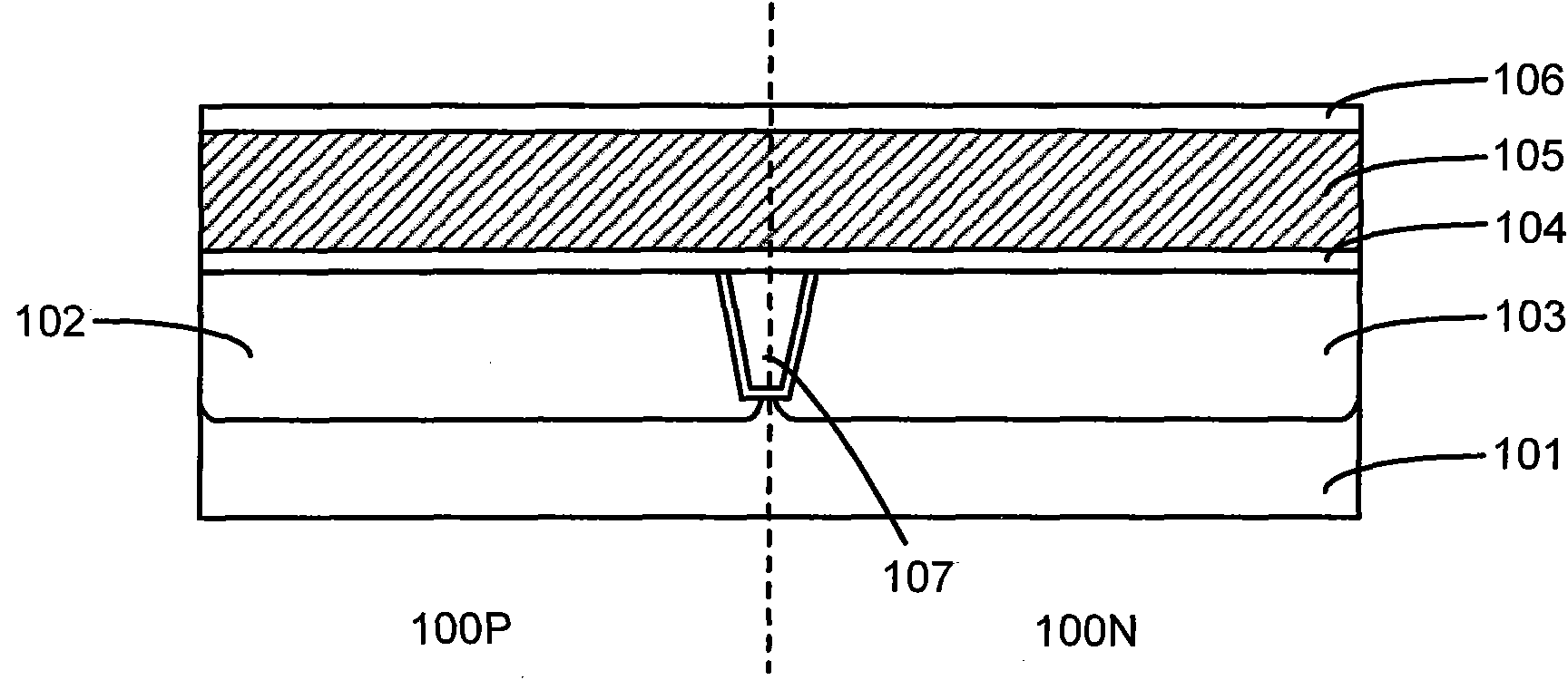
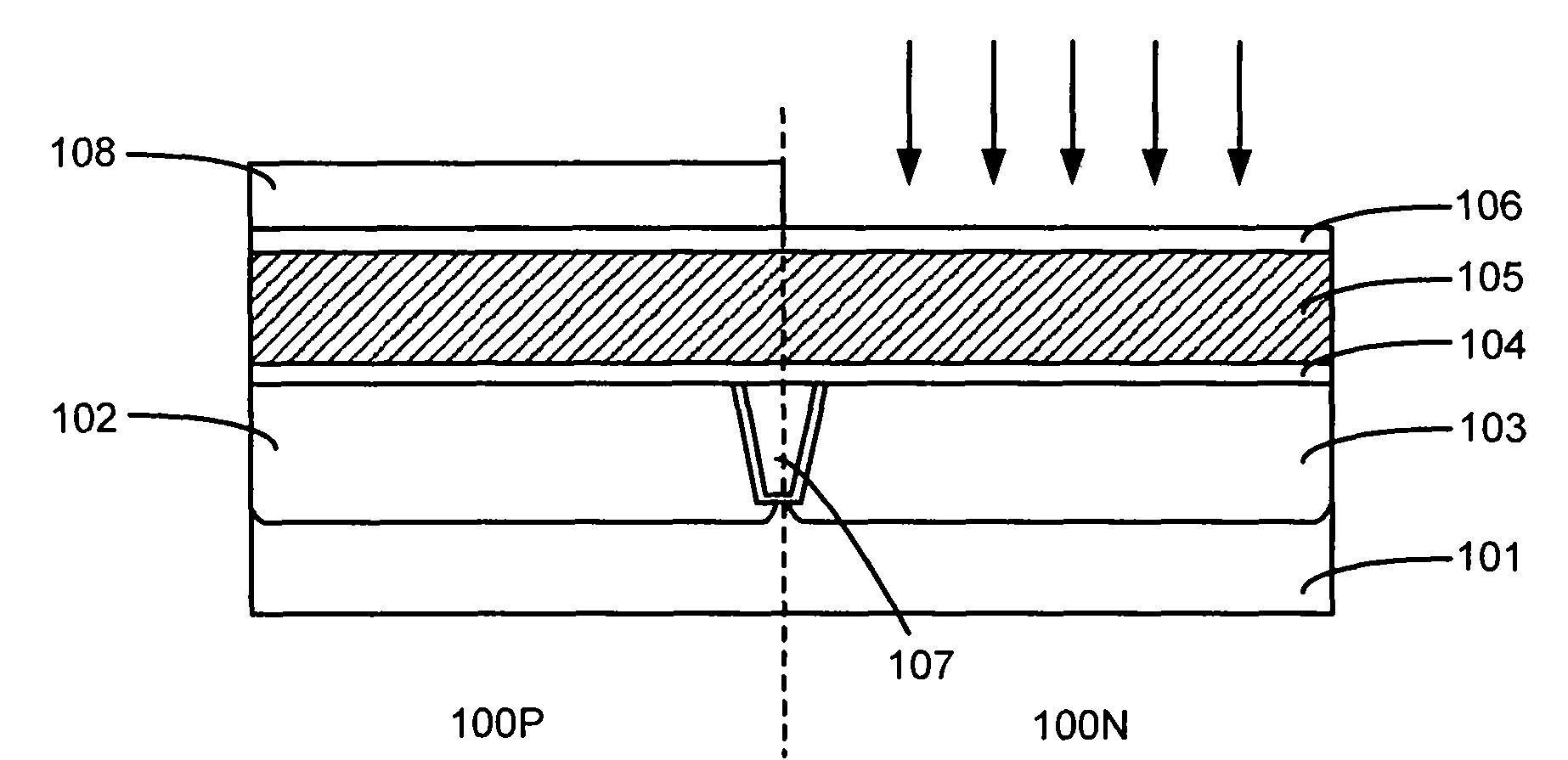
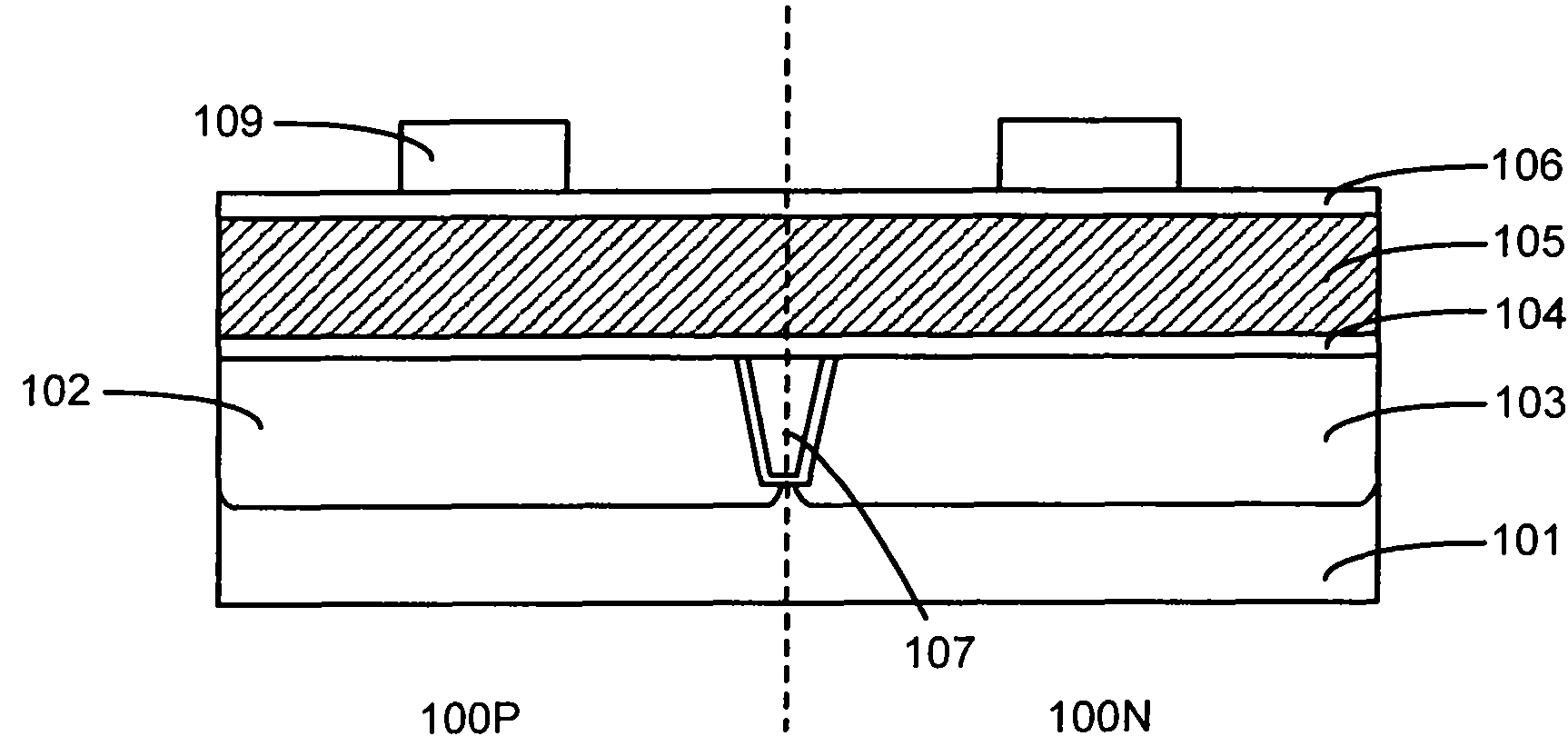
[0040] In order to thoroughly understand the present invention, detailed steps will be presented in the following description to illustrate how the present invention can fabricate a polysilicon gate structure with precise line width and better line edge roughness. Obviously, the implementation of the present invention is not limited to the specific details familiar to those skilled in the semiconductor field. The preferred embodiments of the present invention are described in detail as follows. However, in addition to these detailed descriptions, the present inventi...


PUM


Abstract

The invention provides a method for manufacturing a polycrystalline silicon gate structure. The method comprises the following steps of: providing a front-end device structure, wherein a polycrystalline silicon layer is formed on the front-end device structure and impurities are predoped in the part from the surface to the preset depth of the polycrystalline silicon layer; forming a masking layer on the surface of the polycrystalline silicon layer, and forming a photoinduced resist layer with patterns on the masking layer; taking the photoinduced resist layer as a mask and carrying out first etching on the masking layer and the polycrystalline silicon layer, wherein the etching depth of the polycrystalline silicon layer is larger than the preset depth and is less than the thickness of the polycrystalline silicon layer; removing the photoinduced resist layer; forming side-wall oxidizing layers on the side wall of the masking layer and the side wall of the polycrystalline silicon layer; and taking the masking layer and the side-wall oxidizing layers as masks, and carrying out second etching on the polycrystalline silicon layer till the surface of the front-end device structure is exposed. According to the method, a polycrystalline silicon gate structure with accurate line width and better LER (line edge roughness) can be formed, so that the electric performance of a semiconductor device is improved.

Description

Technical field [0001] The present invention relates to a method for manufacturing a semiconductor device, and in particular, to a method for manufacturing a polysilicon gate structure. Background technique [0002] At present, driven by the demand for miniaturization, high-density, high-speed, high-reliability, and system integration of semiconductor devices, the minimum feature size of semiconductor devices has entered the era of 45nm and below nodes. The composition and structure of the semiconductor device simply scaled down will become infeasible due to excessive leakage. Therefore, while the semiconductor device is scaled down, the leakage will be reduced by changing part of the composition or structure. [0003] As early as when the minimum feature size of semiconductor devices entered the 90nm node era, polysilicon materials were widely used in the production of complementary metal oxide semiconductor field effect transistors (CMOSFETs, due to their better heat resistance a...

Claims


Application Information

Patent Timeline
Patent Type & Authority Patents(China)
IPC IPC(8): H01L21/28H01L21/3213
Inventor 韩秋华孟晓莹
Owner SEMICON MFG INT (SHANGHAI) CORP
Why Eureka
Try Eureka