Negative resist composition

a technology of composition and resist, applied in the field of negative resist composition, can solve the problems of increasing the sensitivities of materials, aggravating line edge roughness, deteriorating pattern profiles, etc., and achieves the effects of enhancing microlithography performance, high sensitivity, and high resolution

Active Publication Date: 2006-08-15
FUJIFILM CORP +1
View PDF9 Cites 2 Cited by
  • Summary
  • Abstract
  • Description
  • Claims
  • Application Information

AI Technical Summary

Benefits of technology

[0007]Therefore, the invention is aimed at solving problems facing the arts of enhancing performances in microlithography for semiconductor devices and, more particularly, providing a negative resist composition which can concurrently satisfy all the characteristics requirements, including high sensitivity, high resolution, good resist pattern profiles and favorable line-edge roughness, notably in electron-beam lithography or X-ray lithography for production of semiconductor devices.

Problems solved by technology

Increasing the sensitivity is a very important problem, notably in reducing a wafer processing time.
As to negative resists for use in electron-beam lithography, however, the pursuit of increases in their sensitivities gives rise to aggravation of line edge roughness in addition to a drop in resolution and a deterioration of pattern profiles.
Transfer of this roughness occurs in the etching process using the resist as a mask, and results in deterioration of electric characteristics and lowering of yields.
Particularly in the superfine region of 0.25 μm or below, an improvement in the line edge roughness is a vitally important problem.
However, those compounds, even when they are used in any combinations, were unsuccessful at concurrently satisfying all the resist-performance requirements in the superfine region, namely high sensitivity, high resolution, good pattern profiles and favorable line-edge roughness.

Method used


Image

  • Negative resist composition
  • Negative resist composition
  • Negative resist composition

Examples


synthesis example 1

Synthesis of Acid-Generator (1-1)

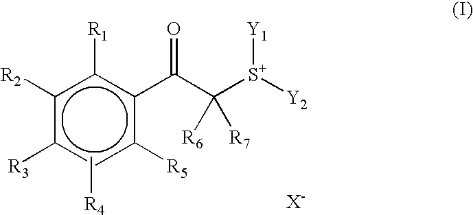
[0215]To a mixture of 16.4 g of AgBF4 with 150 ml of acetonitrile, a solution containing 16.0 g of phenacyl bromide and 12.4 g of di-n-butyl sulfide in 50 ml of acetonitrile was added over a period of 30 minutes. After stirring for one night at room temperature, the reaction solution was concentrated to deposit a powder. The powder was washed with diisopropyl ether to give 27 g of phenacyldi-n-butylsulfonium tetrafluoroborate.

[0216]The phenacyldi-n-butylsulfonium tetrafluoroborate in an amount of 10 g was dissolved in 200 ml of methanol, and thereto 10.1 g of potassium nonafluorobutanesulfonate was added and stirred for one hour at room temperature. The reaction solution thus obtained was mixed with 500 ml of chloroform, and washed with two 300 ml portions of distilled water. The organic layer was concentrated to yield 9.8 g of an acid generator (1-1).

[0217]The other compounds were synthesized in similar manners to the above.

2. EXAMPLES

example 1

(1) Preparation and Coating of Negative Resist Solution:

[0218]

Resin (29) (Component (A))0.70 gCross-linking agent MM-1 (Component (B))0.25 gAcid generator I-1 (Component (C))0.05 g

[0219]The above ingredients were dissolved in 8.5 g of propylene glycol monomethyl ether acetate, and therein 0.002 g of OE-1 as Component (D) was mixed and dissolved. Further therein, 0.001 g of Megafac F176 (a product of Dainippon Ink & Chemicals, Inc., hereinafter abbreviated as “W-1”) as a surfactant was mixed and dissolved. The solution obtained was subjected to fine filtration with a membrane filter 0.1 μm in pore diameter, thereby preparing a negative resist solution.

[0220]The thus prepared negative resist solution was coated on a 6-inch wafer by means of a spin coater Mark 8 made by Tokyo Electron, and dried for 90 seconds on a 110° C. hot plate to form a resist film having a thickness of 0.3 μm.

(2) Formation of Negative Resist Patterns:

[0221]The resist film is irradiated with an electron-beam draw...

examples 2 to 30

[0227]Using various combinations of ingredients as shown in Tables 1 to 3, negative resist solutions were prepared and negative patterns were formed in the same manner as in Example 1. The evaluation results are shown in Tables 4 and 5.


PUM

PropertyMeasurementUnit
roughnessaaaaaaaaaa
molecular weight distributionaaaaaaaaaa

Abstract

A negative resist composition comprising (A) an alkali-soluble polymer, (B) a cross-linking agent forming cross-links between molecules of the alkali-soluble polymer (A) under the action of an acid and (C) a specified acid generator, which can satisfy all of performance requirements concerning sensitivity, resolution, pattern profile and line-edge roughness in the pattern formation by irradiation with electron beams or X-rays.

Description

FIELD OF THE INVENTION[0001]The present invention relates to a negative resist composition used suitably in supermicrolithography and other fabrication processes for production of VLSIs and high-capacity microchips. More specifically, the invention is concerned with a negative resist composition capable of forming highly resolved patterns by using electron beams or X-rays in particular.BACKGROUND OF THE INVENTION[0002]In processes of producing semiconductor devices, such as ICs and LSIs, fine patterning has so far been performed by photoresist composition-utilized lithography. With recent increase in packing densities of chips, there has been a growing demand for formation of superfine patterns having their widths in the region of submicrons or quatermicrons. In line with such a demand, there has been a trend toward exposure light of shorter wavelengths, namely a trend to change exposure light from g-ray to i-ray and further to KrF excimer laser light. At present, development of not...

Claims


Application Information

Patent Timeline
Patent Type & Authority Patents(United States)
IPC IPC(8): G03F7/038C08F12/24C08F20/30C08F20/58G03F7/004H01L21/027
CPCG03F7/0382G03F7/0045
Inventor YASUNAMI, SHOICHIROKODAMA, KUNIHIKO
Owner FUJIFILM CORP
Why Eureka
Try Eureka