Silicon photonics connector
- Summary
- Abstract
- Description
- Claims
- Application Information
AI Technical Summary
Benefits of technology
Problems solved by technology
Method used
Image

Examples
Embodiment Construction
Overview
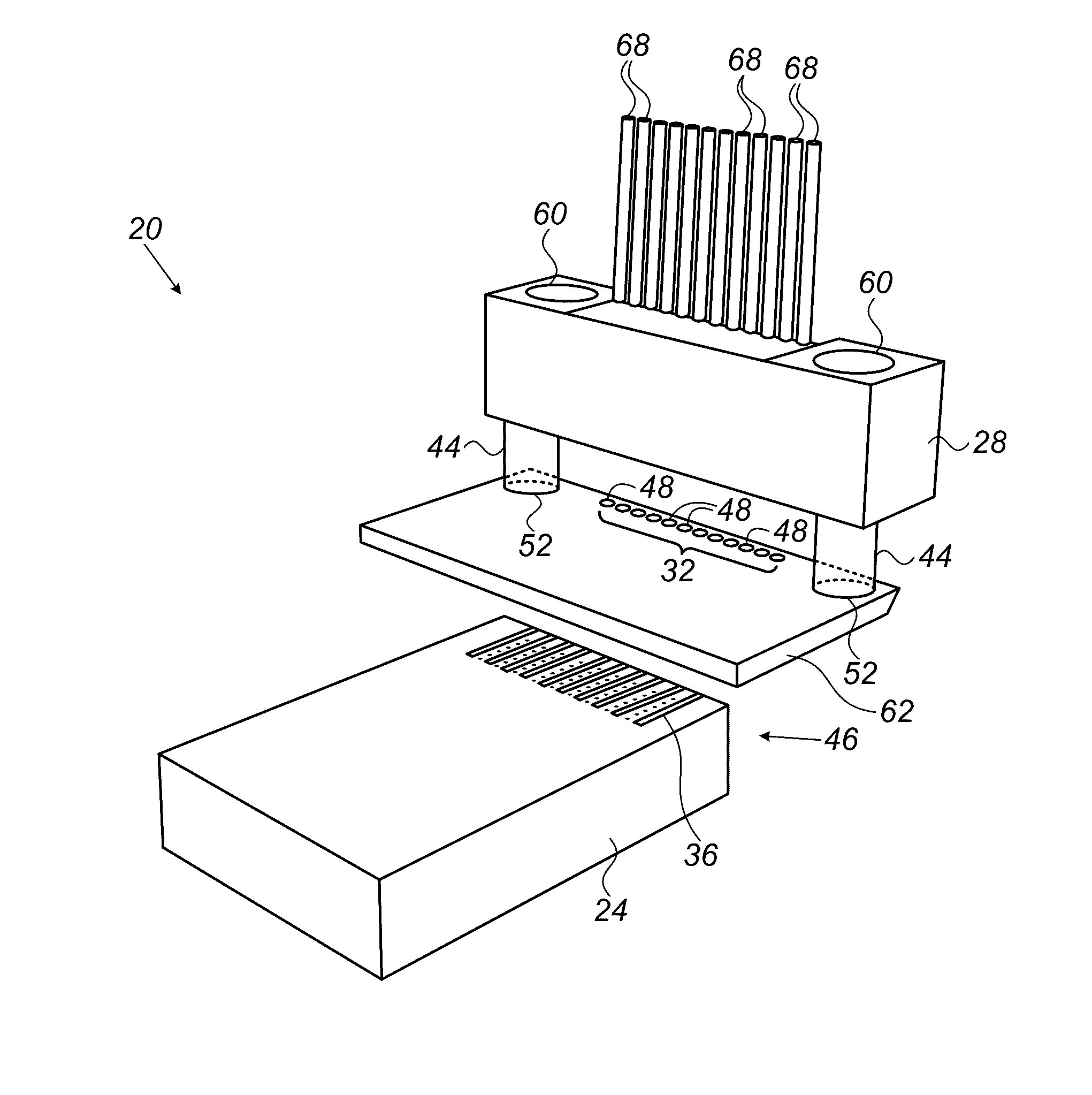
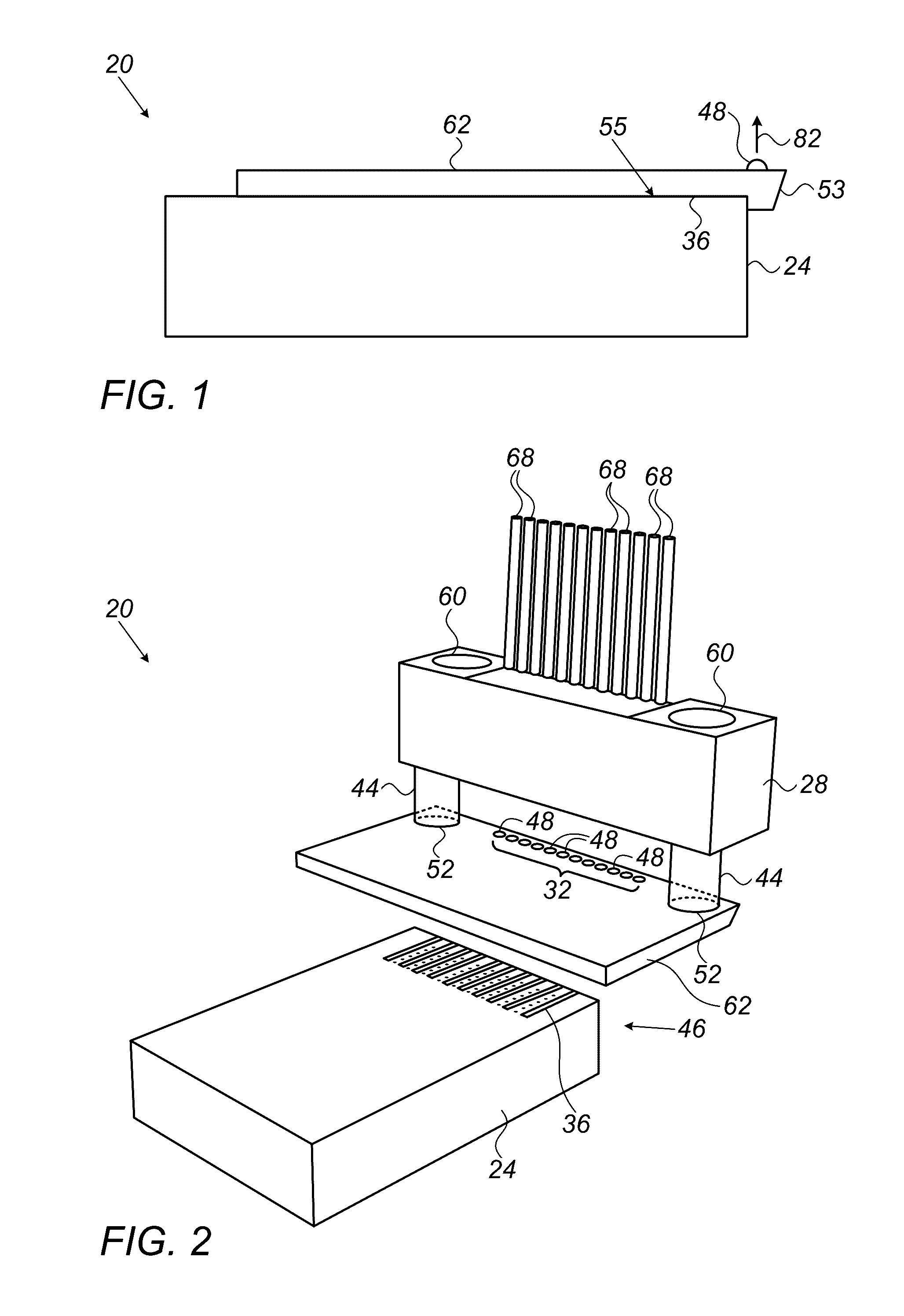
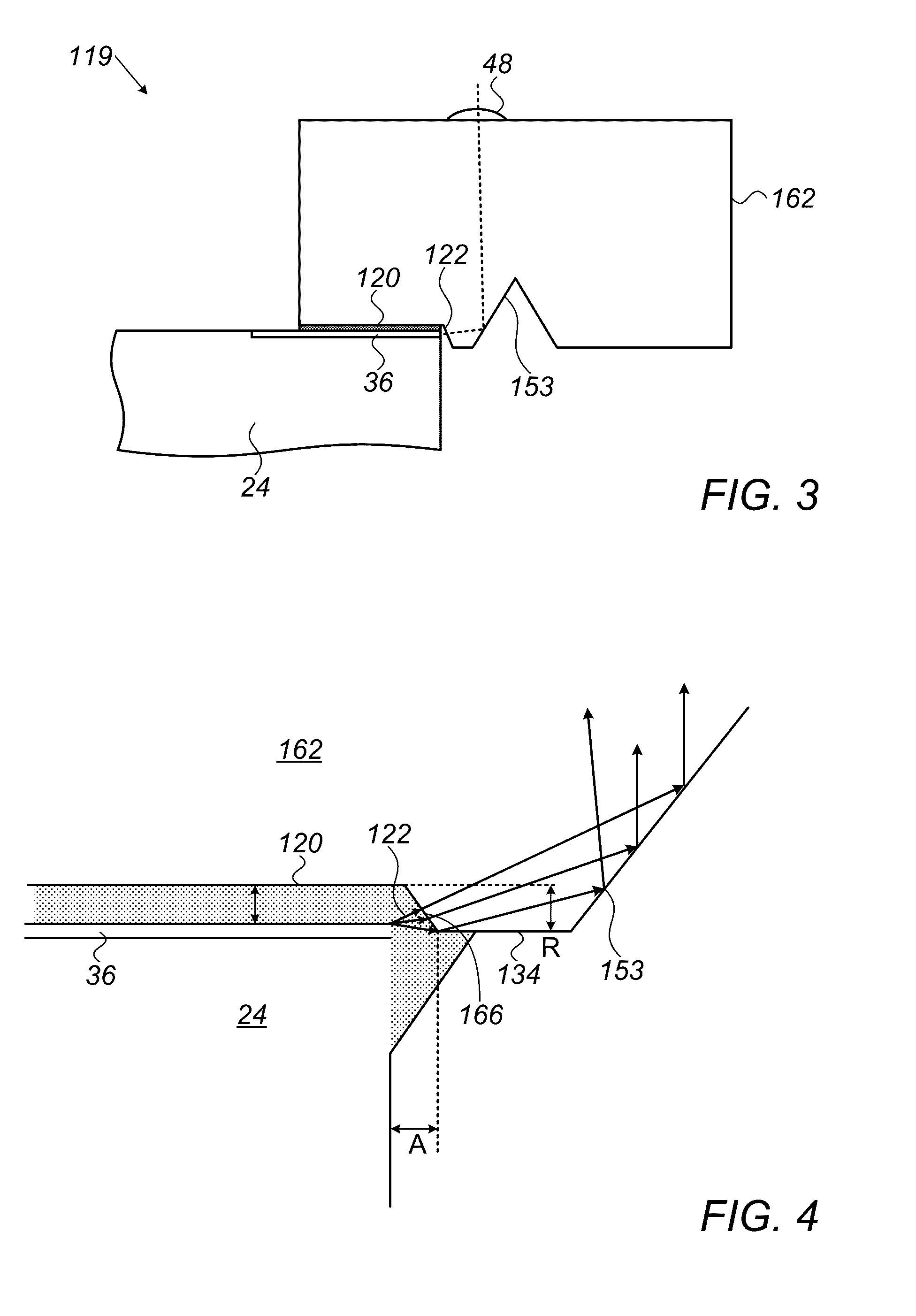
[0046]Interconnection between Silicon Photonics (SiP) devices and external optical signal carriers is technologically challenging, because of the accuracy required for the alignment of light beams. SiP waveguides typically have a diameter on the order of 3 μm, for example between 0.1 and 3 micrometers, which makes a misalignment of even less than 1 micron very problematic.
[0047]Embodiments of the present invention that are described herein provide improved methods and apparatus for interconnecting light from waveguides of SiP devices to other optical elements.
[0048]In an aspect of some embodiments of the invention, the interconnection between the waveguides and external optical elements is performed by an optical system, separate from the SiP device, which deflects the light from the SiP device waveguides by an angle of at least 30° or even at least 60°, for example by about 90°. Optionally, the light exiting the waveguides of the SiP are in a first plane and the light is de...
PUM
 Abstract
Description
Claims
Application Information
 - R&D Engineer
- R&D Manager
- IP Professional
- Industry Leading Data Capabilities
- Powerful AI technology
- Patent DNA Extraction
Browse by: Latest US Patents, China's latest patents, Technical Efficacy Thesaurus, Application Domain, Technology Topic.
© 2024 PatSnap. All rights reserved.Legal|Privacy policy|Modern Slavery Act Transparency Statement|Sitemap