Substrate-guided optical devices

a technology of optical devices and substrates, applied in the field of substrate-guided optical devices, can solve the problems of high cost where high-performance is required, inconvenient installation, unsafe use, etc., and achieve the effect of convenient incorporation and convenient structure and fabrication of compact devices

Active Publication Date: 2007-04-26
LUMUS LTD
View PDF8 Cites 129 Cited by
  • Summary
  • Abstract
  • Description
  • Claims
  • Application Information

AI Technical Summary

Benefits of technology

[0005] The present invention facilitates the structure and fabrication of very compact light-guide optical elements (LOE) for, amongst other applications, head-mounted displays. The invention allows relatively wide FOV's together with relatively large EMB values. The resulting optical system offers a large, high-quality image, which also accommodates large movements of the eye. The optical system offered by the present invention is particularly advantageous because it is substantially more compact than state-of-the-art implementations and yet it can be readily incorporated, even into optical systems having specialized configurations.

Problems solved by technology

Nevertheless, state-of-the-art HUD's suffer several significant drawbacks.
As a result, the combiner-projector HUD system is necessarily bulky and large, and requires considerable installation space, making it inconvenient for installation and, at times, even unsafe to use.
The large optical aperture of conventional HUDs also pose a significant optical design challenge; rendering the HUD's with either a compromising performance, or leading to high cost wherever high-performance is required.
The limiting factor remains the quality of the display within the end-user's device.
The mobility requirement restricts the physical size of the displays, and the result is a direct-display with a poor image viewing quality.

Method used


Image

  • Substrate-guided optical devices
  • Substrate-guided optical devices
  • Substrate-guided optical devices

Examples


Embodiment Construction

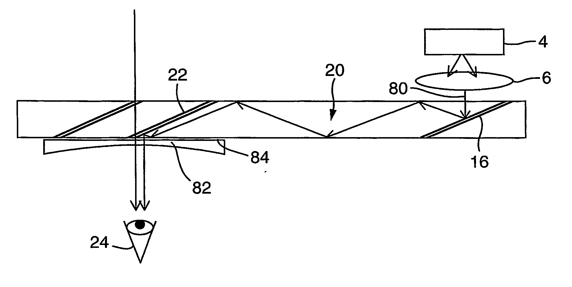
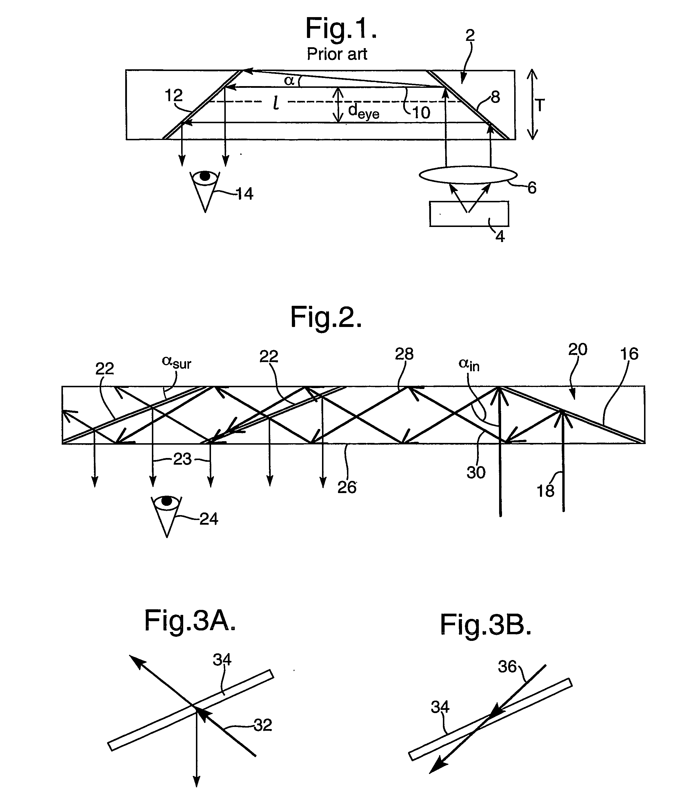
[0030]FIG. 1 illustrates a conventional folding optics arrangement, wherein the substrate 2 is illuminated by a display source 4. The display is collimated by a collimating lens 6. The light from the display source 4 is coupled into substrate 2 by a first reflecting surface 8, in such a way that the main ray 10 is parallel to the substrate plane. A second reflecting surface 12 couples the light out of the substrate and into the eye of a viewer 14. Despite the compactness of this configuration, it suffers significant drawbacks; in particular only a very limited FOV can be affected. As shown in FIG. 1, the maximum allowed off-axis angle inside the substrate is: αmax=arctan⁡(T-deye2⁢l),(1)

wherein T is the substrate thickness;

[0031] deye is the desired exit-pupil diameter, and

[0032] l is the distance between reflecting surfaces 8 and 12.

[0033] With angles higher than αmax the rays are reflected from the substrate surface before arriving at the reflecting surface 12. Hence, the refl...


PUM


Abstract

There is provided an optical device, having a light-transmitting substrate (20) having at least two major surfaces parallel to each other and edges; a display light source; optical means for coupling light from the light source into the substrate (20) by internal reflection, and at least one partially reflecting surface (22) located in the substrate (20) which is non-parallel to the major surfaces of the substrate wherein the source emits light waves located in a given field-of-view, that the light waves are collimated, that an angular resolution is defined for the optical device, and wherein the angular deviation between any two different rays located in one of the collimated light waves, is smaller than the angular resolution.

Description

[0001] The present invention relates to substrate-guided optical devices, and particularly to devices which include a plurality of reflecting surfaces carried by a common light-transmissive substrate, also referred to as a light-guide. [0002] The invention can be implemented to advantage in a large number of imaging applications, such as, for example, head-mounted and head-up displays (HMD's and HUD's), cellular phones, compact displays, 3-D displays, compact beam expanders, as well as non-imaging applications such as flat-panel indicators, compact illuminators and scanners. BACKGROUND OF THE INVENTION [0003] One of the important applications for compact optical elements is in HMD's wherein an optical module serves both as an imaging lens and a combiner, in which a two-dimensional display is imaged to infinity and reflected into the eye of an observer. The display can be obtained directly from either a spatial light modulator (SLM) such as a cathode ray tube (CRT), a liquid crystal ...

Claims


Application Information

Patent Timeline
Patent Type & Authority Applications(United States)
IPC IPC(8): G02B27/14F21V8/00G02B6/00G02B27/00G02B27/01G02B27/02G02B27/28
CPCG02B6/00G02B6/0035G02B6/0056G02B27/0081G02B27/0101G02B27/0172G02B27/02G02B27/28G02B2027/0114G02B2027/0116G02B2027/0118G02B2027/012G02B2027/0125G02B2027/0132G02B2027/0178G02C7/086
Inventor AMITAI, YAAKOV
Owner LUMUS LTD
Why Eureka
Try Eureka