Oscillation element and oscillator using the same

a technology of oscillator and oscillator, which is applied in the direction of oscillator generator, network simulating negative resistance, electrical apparatus, etc., can solve the problems of complex design and attenuation of oscillation at the desired frequency

Active Publication Date: 2016-12-22
CANON KK
View PDF2 Cites 5 Cited by
  • Summary
  • Abstract
  • Description
  • Claims
  • Application Information

AI Technical Summary

Benefits of technology

[0008]According to an aspect of the present invention, there is provided an oscillation element that oscillates an electromagnetic wave, the oscillation element including: a negative resistance element; and a resonator including a first conductor and a second conductor, in which the negative resistance element and the resonator are arranged on a substrate, the negative resistance element is electrically connected to the first conductor and the second conductor, the first conductor and the second conductor are capacitively coupled to each other, and when a capacitance between the first conductor and the second conductor is set as C, an inductance of the first conductor and the second conductor is set as L1, a speed of the oscillated electromagnetic wave in vacuum is set as CC, a relative dielectric constant of the substrate is set as Er, and a length of a diagonal line of the substrate is set as d, a series resonant frequency f1 of the resonator satisfies f1=1 / {2π√(L1C)}, and

Problems solved by technology

For that reason, the design may be complicated, or the oscillation at the desired frequency may also be attenuated.

Method used


Image

  • Oscillation element and oscillator using the same
  • Oscillation element and oscillator using the same
  • Oscillation element and oscillator using the same

Examples


first exemplary embodiment

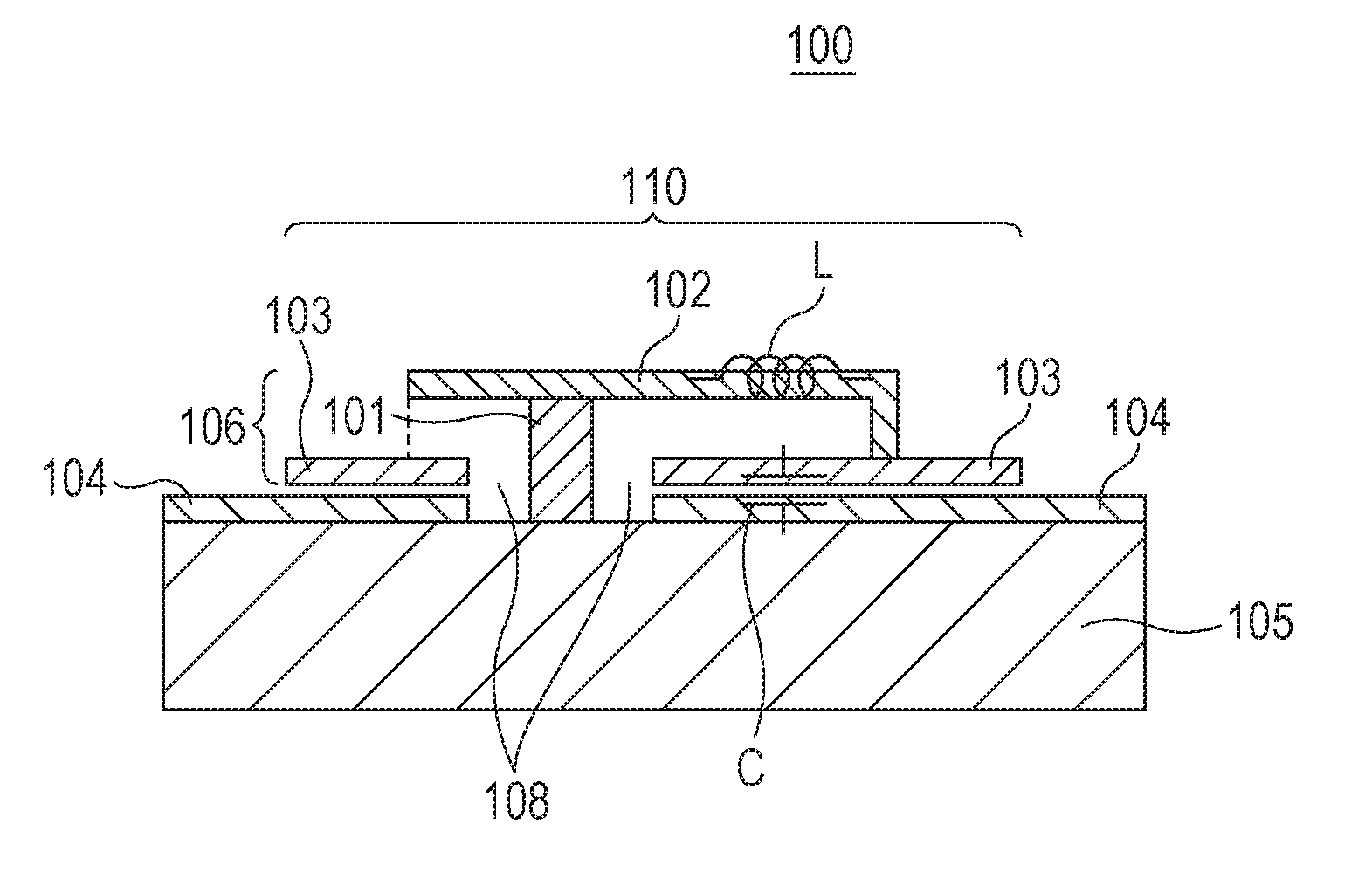
[0027]An oscillator that oscillates a terahertz wave includes an oscillation element provided with a negative resistance element and a resonator of a distributed constant type, and a power supply that supplies a bias voltage to the negative resistance element. The bias voltage from the power supply is supplied to the negative resistance element via a bias supply unit including an electric wire and a conductor. A parasitic low-frequency oscillation (parasitic oscillation) in the terahertz wave oscillator is generated in many cases because of a structure accompanied by this bias supply unit. Therefore, the bias supply unit is caused to have a characteristic in an oscillation element 100 according to the present exemplary embodiment. That is, a structure is adopted where a part of the bias supply unit is included in a part of a resonator 110 of a distributed constant type and is also capacitively coupled thereto.

[0028]Therefore, the bias supply unit is caused to have a characteristic i...

second exemplary embodiment

[0057]An oscillation element 200 according to the present exemplary embodiment will be described by using FIG. 4. FIG. 4 is a cross sectional view of the oscillation element (semiconductor die) 200.

[0058]The oscillation element 200 includes a negative resistance element 201 (hereinafter, will be referred to as “element 201”) and a resonator 210. The element 201 and the resonator 210 are arranged on a substrate 205. The resonator 210 includes a first conductor 206 (hereinafter, will be referred to as “conductor 206”) which includes a first conductive layer 202 (hereinafter, will be referred to as “conductive layer 202”), and also a second conductive layer 203 (hereinafter, will be referred to as “conductive layer 203”) and a second conductor 204 (hereinafter, will be referred to as “conductor 204”) provided with a third conductive layer. The element 201 is electrically connected to each of the conductors 204 and 206. It is noted that the conductor 204 may be referred to as the conduc...

example 1

[0073]An oscillator 350 according to Example 1 will be described. FIG. 6A is a schematic diagram of the oscillator 350, and FIG. 6B is a cross sectional view of the oscillation element.

[0074]The oscillator 350 uses resonant tunneling diodes as negative resistance elements 301a and 301b. According to the present example, since two resonators 310 of the distributed constant type are used, two RTD 301a and 301b are provided. The resonators 310 each include a first conductor 306 (hereinafter, will be referred to as “conductor 306”) and a second conductor 304 (hereinafter, will be referred to as “conductor 304”).

[0075]A first conductive layer 302, a second conductive layer 303, and the third conductive layer (second conductor) 304 are each a metallic layer using Ti / Pd / Au metal having a thickness of 200 nm. Hereinafter, these conductive layers are respectively referred to as metallic layer (first metallic layer) 302, metallic layer (second metallic layer) 303, and metallic layer (third me...


PUM


Abstract

An oscillation element that oscillates an electromagnetic wave includes a negative resistance element and a resonator including a first conductor and a second conductor, in which the negative resistance element and the resonator are arranged on a substrate, the negative resistance element is electrically connected to the first conductor and the second conductor, the first conductor and the second conductor are capacitively coupled to each other, and when a capacitance between the first conductor and the second conductor is set as C, an inductance of the first conductor and the second conductor is set as L1, a speed of the oscillated electromagnetic wave in vacuum is set as CC, a relative dielectric constant of the substrate is set as εr, and a diagonal line length of the substrate is set as d, a series resonant frequency f1 of the resonator satisfies f1=1/{2π√(L1C)}, and f1<Co/[d·{(1+εr)/2}].

Description

TECHNICAL FIELD[0001]The present invention relates to an oscillation element including a negative resistance element and an oscillator using this oscillation element.BACKGROUND ART[0002]A negative resistance element involves a resonator and is useful in an application field of an electromagnetic wave oscillation element. Up to now, it has been proposed that an electromagnetic wave including at least a part of a frequency band from a millimeter waveband to a terahertz band (which is higher than or equal to 30 GHz and lower than or equal to 30 THz) (hereinafter, will be simply referred to as “terahertz wave”) can be generated by using the negative resistance element. As one of the configurations, NPL 1 discloses a monolithic oscillator obtained by integrating the negative resistance element and the resonator to each other on a substrate. Slot antennas are integrated to each other on a semiconductor substrate including the negative resistance element, and a resonator structure and a ga...

Claims


Application Information

Patent Timeline
Patent Type & Authority Applications(United States)
IPC IPC(8): H03B7/12H03B7/08
CPCH03B7/08H03B7/12H03H7/1741H03B9/12H03H7/0123H03H7/383H03H11/52
Inventor SEKIGUCHI, RYOTA
Owner CANON KK
Why Eureka
Try Eureka