Light emitting element and light emitting device

Active Publication Date: 2017-01-19
NICHIA CORP
View PDF1 Cites 6 Cited by
  • Summary
  • Abstract
  • Description
  • Claims
  • Application Information

AI Technical Summary

Benefits of technology

This patent aims to improve the brightness and evenness of light emitting elements and devices. By reducing unevenness in current density, the technical effects of the patent can enhance the overall light emission intensity distribution.

Problems solved by technology

On the other hand, in a light emitting element, the current density is greater in a region where the distance between an anode electrode (a p-side electrode) and a cathode electrode (an n-side electrode) is short, which tends to result in uneven light emission.

Method used


Image

  • Light emitting element and light emitting device
  • Light emitting element and light emitting device
  • Light emitting element and light emitting device

Examples


first embodiment

Structure of Light Emitting Device

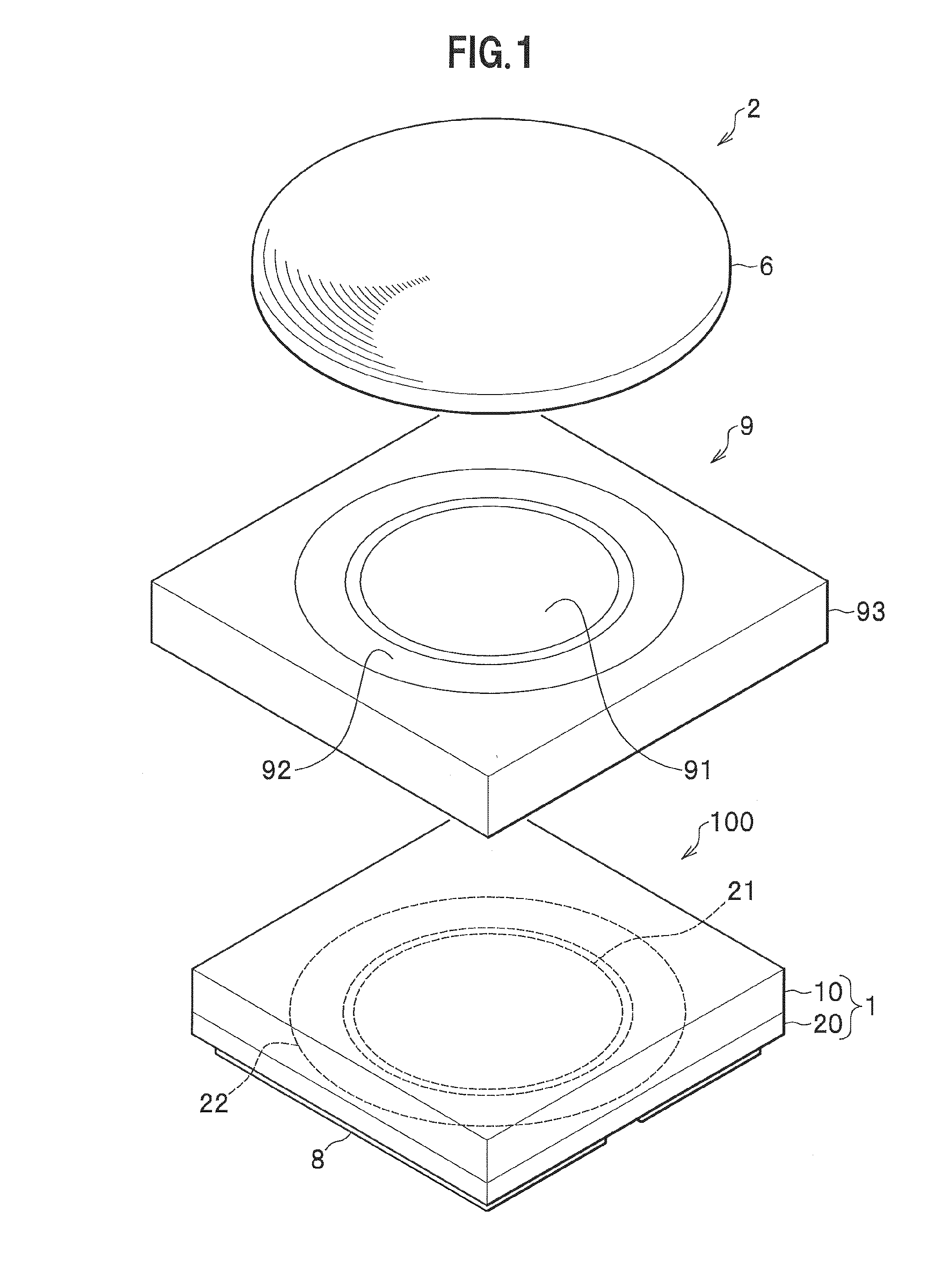
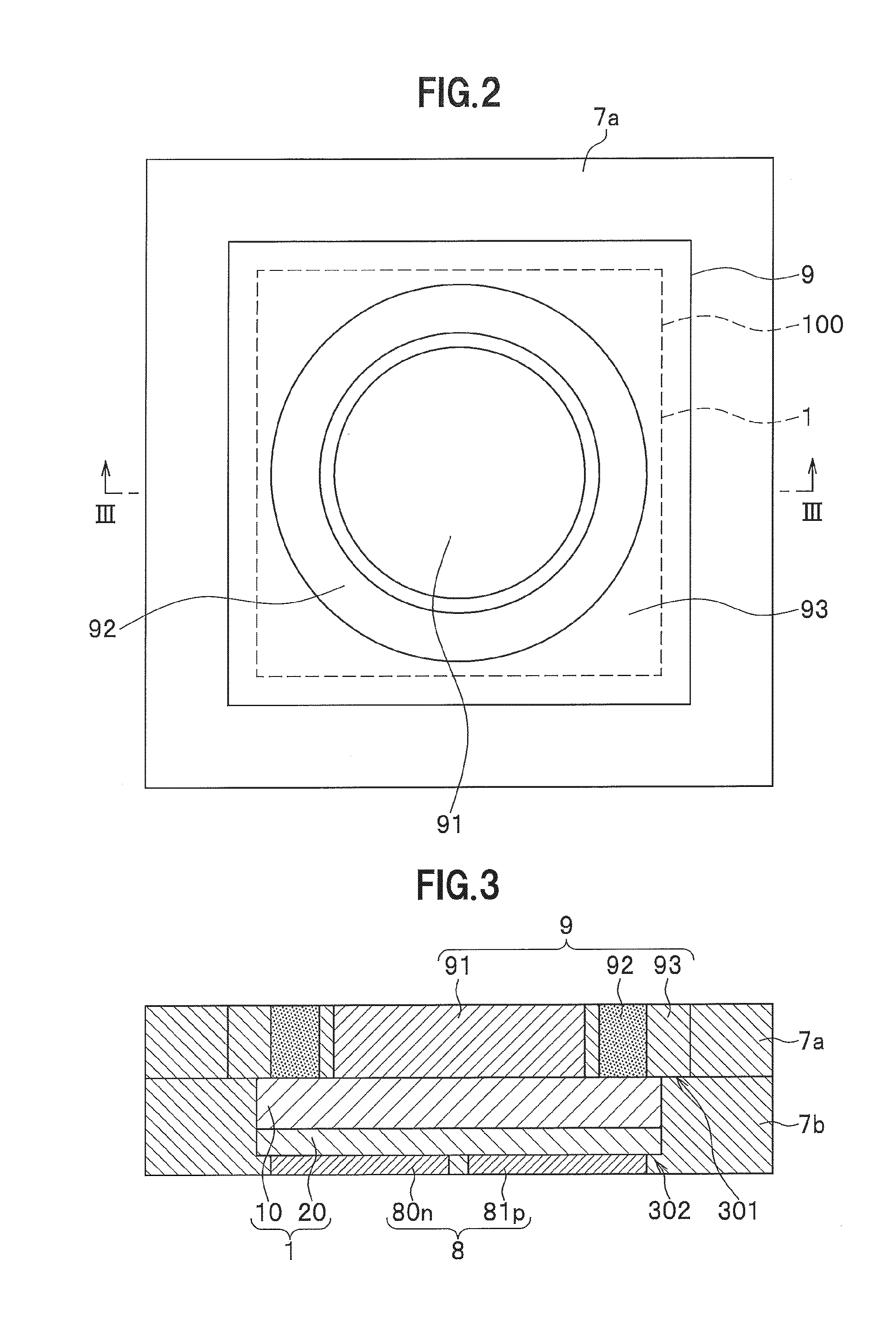
[0035]Firstly, with reference to FIGS. 1 to 4, a description will be given of the structure of a light emitting element and a light emitting device according to a first embodiment of the present invention. A light source 2 shown in FIG. 1 includes a light emitting device 100, a wavelength conversion member 9 provided on a light-transmissive substrate 10 side of the light emitting device 100, and a Fresnel lens 6 provided opposite to the light-transmissive substrate 10 with reference to the wavelength conversion member 9. The light source 2 may be used as illumination, or may be installed in an external apparatus unit such as a flash module of a camera, for example. An exemplary external apparatus unit may be a camera-equipped mobile terminal such as a smartphone.

[0036][Light Emitting Device]

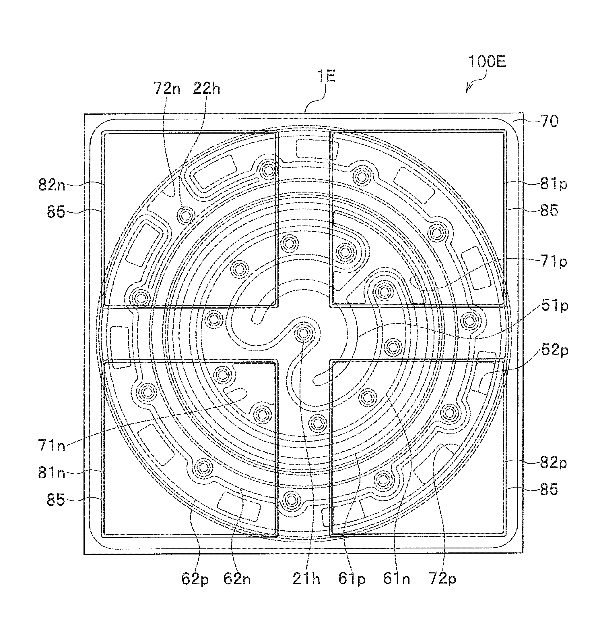
[0037]The light emitting device 100 includes a light emitting element 1 and external connection electrodes 8. The light emitting device 100 is packaged having it...

second embodiment

[0160]As shown in FIGS. 13 and 14, a light emitting element 1B and a light emitting device 100B according to the second embodiment are different from the light emitting element 1 and the light emitting device 100 according to the first embodiment in the openings of the interlayer insulating film 50. In the following, constituent members similar to those of the light emitting device 100 are denoted by like reference characters, and the description thereof will not be repeated.

[0161]The light emitting device 100B includes the light emitting element 1B, the external connection electrodes 8 (the n-side external connection electrode 80n, the first p-side external connection electrode 81p, and the second p-side external connection electrode 82p).

[0162]In the light emitting element 1B, the interlayer insulating film 50 includes n-side openings 53n on the outer circumference side of the second semiconductor region 22 (left in FIG. 14). Herein, the outer edge portion 22s of the n-type semico...

third embodiment

[0165]As shown in FIGS. 15 and 16, a light emitting element 1C and a light emitting device 100C according to a third embodiment are different from the light emitting element 1 and the light emitting device 100 according to the first embodiment in including two semiconductor stacked-layer bodies. In the following, constituent members similar to those of the light emitting device 100 are denoted by like reference characters, and the description thereof will not be repeated.

[0166]The light emitting device 100C includes the light emitting element 1C, and the external connection electrodes 8 (the n-side external connection electrode 80n, the first p-side external connection electrode 81p, and the second p-side external connection electrode 82p).

[0167]In the first embodiment, the n-type semiconductor layer is continuously formed across the first semiconductor region 21 and the second semiconductor region 22. On the other hand, in the third embodiment, the n-type semiconductor layer is sep...


PUM


Abstract

Provided are a light emitting element and a light emitting device with improved light emission intensity distribution. A light emitting element includes a light-transmissive substrate, an n-type semiconductor layer, a first p-type semiconductor layer, a first p-side electrode, a first n-side electrode, a second p-type semiconductor layer, a second p-side electrode, and a second n-side electrode. A light emitting device includes the light emitting element, and an external connection electrode provided at the light emitting element on a side opposite to the light-transmissive substrate. The external connection electrode includes an n-side external connection electrode connected to the first n-side electrode and the second n-side electrode, a first p-side external connection electrode connected to the first p-side electrode, and a second p-side external connection electrode connected to the second p-side electrode.

Description

CROSS-REFERENCE TO RELATED APPLICATIONS[0001]The present application claims priority under 35 U. S. C. §119 to Japanese Patent Application No. 2015-142461, filed Jul. 16, 2015, and Japanese Patent Application No. 2016-135407, filed Jul. 7, 2016. The contents of these applications are incorporated herein by reference in their entireties.BACKGROUND[0002]1. Technical Field[0003]The present disclosure relates to a light emitting element and a light emitting device.[0004]2. Description of Related Art[0005]In the field of light emitting elements used in light emitting devices, various development efforts have conventionally been made for achieving an even light emission intensity distribution in a light extraction surface. For example, a light emitting element used in a light emitting device disclosed in WO2009 / 019836 has at least two regions, namely, an edge portion and a region inner than the edge portion. The light emitting element is provided with an anode electrode at each of the edg...

Claims


Application Information

Patent Timeline
IPC IPC(8): H01L33/58H01L33/24H01L33/60H01L33/50H01L33/38H01L33/40
CPCH01L33/58H01L33/387H01L33/24H01L33/60H01L33/504H01L33/40H01L33/382
Inventor EMURA, KEIJIINOUE, YOSHIKIKAGEYAMA, HIROAKI
Owner NICHIA CORP
Why Eureka
Try Eureka