SELF SHIELDED SYSTEM IN PACKAGE (SiP) MODULES

Active Publication Date: 2017-01-26
APPLE INC
View PDF4 Cites 20 Cited by
  • Summary
  • Abstract
  • Description
  • Claims
  • Application Information

AI Technical Summary

Benefits of technology

[0015]In certain embodiments, the metal shield is electrically coupled to a ground layer in the PCB to form an EMI shield around the SiP. The EMI shield may inhibit EMI or other electrical interference on the components within the SiP. In certain embodiments, the metal shield is coupled to at least some metallization along vertical walls in the end portions of the substrate. The metallization along the vertical walls in the end portions of the substrate may be via metallization from through-metal vias formed through a common substrate that remains after singulation of the common substrate to form the SiP. The substrate of the SiP may be a portion of the common substrate remaining after singulation.
[0016]In certain embod

Problems solved by technology

A drawback to SiPs is that any defective chip in the package will result in a non-functional packaged integrated circuit, even if all the remaining modules in the same package are functional.
Mutual inductance between two radiated electromagnetic fields may result in EMI.
Due to EMI, the electromagnetic field around the conductor is no longer evenly distributed (e.g., resulting in skin effects, proximity effects, hysteresis losses, transients, voltage drops, electromagnetic disturbances, EMP/HEMP, eddy current losses, harmonic distortion, and reduction in the permeability of the material).
The chips on these boards are so close to each other that the chances of conduct

Method used


Image

  • SELF SHIELDED SYSTEM IN PACKAGE (SiP) MODULES
  • SELF SHIELDED SYSTEM IN PACKAGE (SiP) MODULES
  • SELF SHIELDED SYSTEM IN PACKAGE (SiP) MODULES

Examples


Embodiment Construction

[0036]This specification includes references to “one embodiment” or “an embodiment.” The appearances of the phrases “in one embodiment” or “in an embodiment” do not necessarily refer to the same embodiment, although embodiments that include any combination of the features are generally contemplated, unless expressly disclaimed herein. Particular features, structures, or characteristics may be combined in any suitable manner consistent with this disclosure.

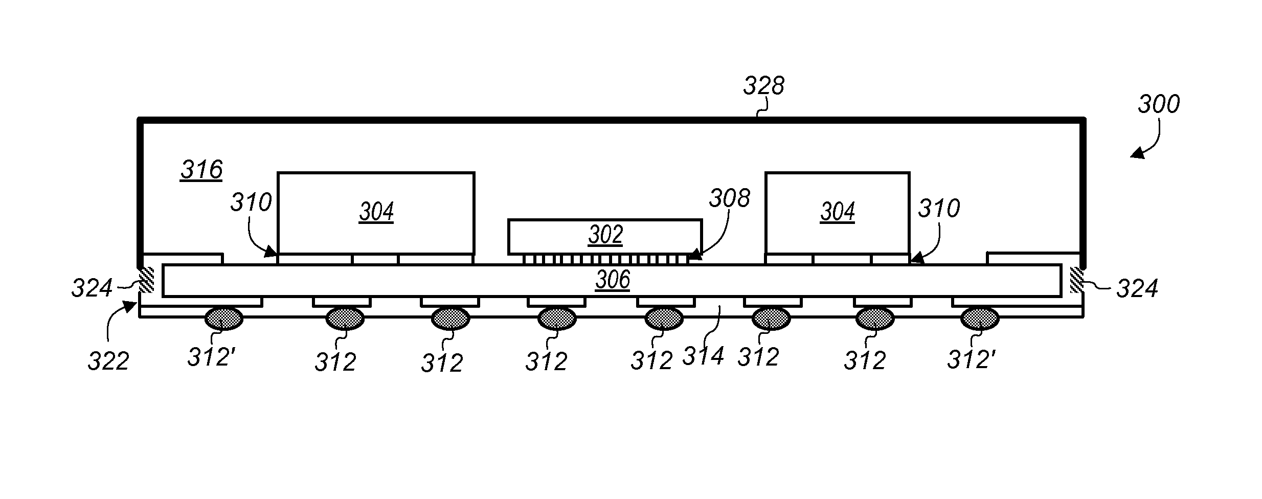
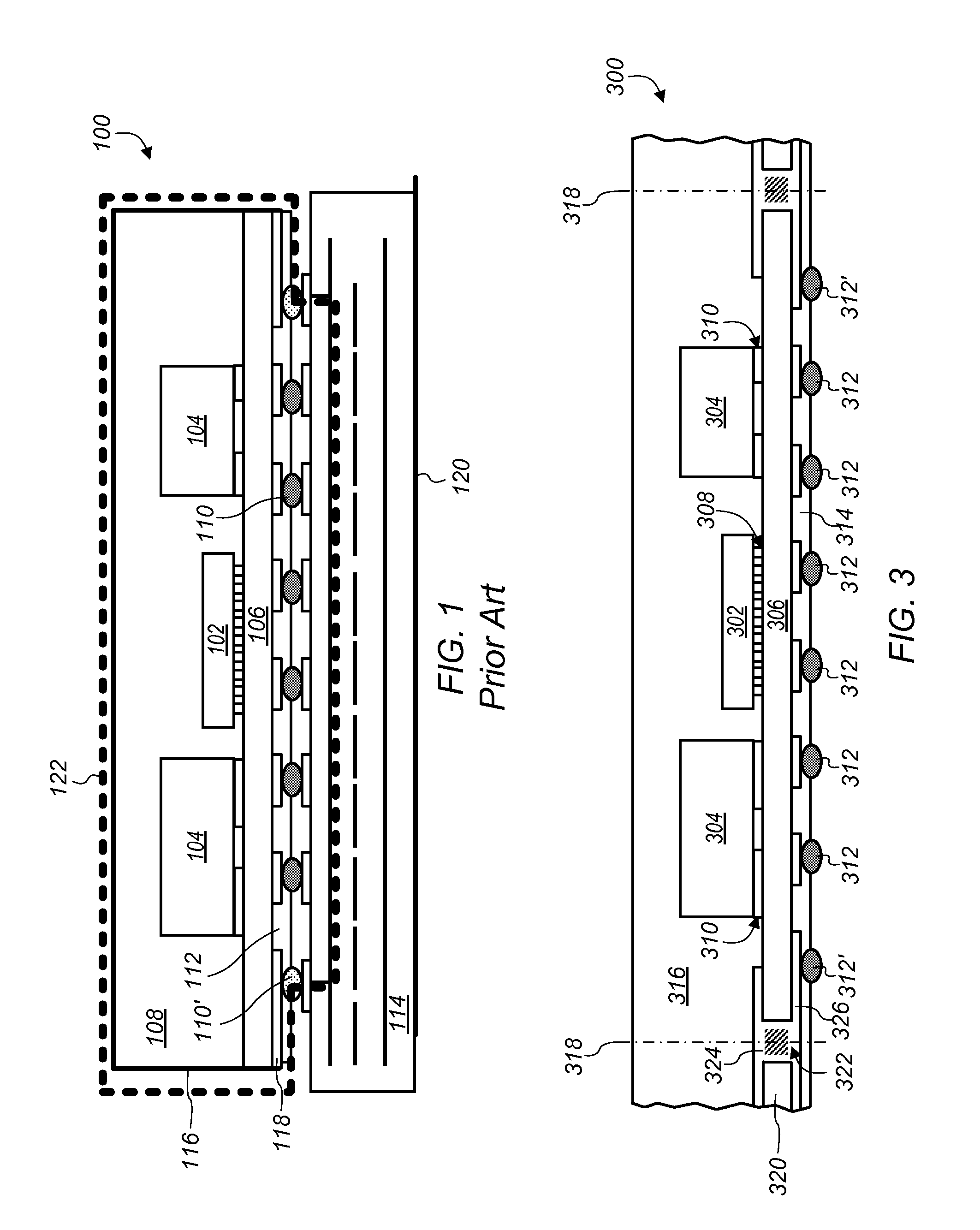
[0037]FIG. 3 depicts a side-view cross-sectional representation of an embodiment of a system in package (SiP). In certain embodiments, SiP 300 includes die 302 and passive devices 304 coupled to an upper surface of substrate 306. In some embodiments, SiP 300 includes only passive devices 304 (e.g., the SiP is a passive SiP). In some embodiments, SiP 300 includes more than one die 302. Die 302 may include, for example, silicon die or integrated circuit die such as processor die or logic die. In some embodiments, die 302 include DRAM...


PUM


Abstract

A system in package (SiP) is disclosed that uses an EMI shield to inhibit EMI or other electrical interference on the components within the SiP. A metal shield may be formed over the SiP. The metal shield may be electrically coupled to a ground layer in a printed circuit board (PCB) to form the EMI shield around the SiP. The substrate of the SiP may include at least some metallization along vertical walls in the end portions of the substrate. The metallization may provide a large contact area for coupling the metal shield to a ground ring coupled to the ground layer in the PCB. The metallization along the vertical walls in the end portions of the substrate may be formed as through-metal vias in a common substrate before singulation to form the SiP.

Description

PRIORITY CLAIM[0001]This patent claims priority to U.S. Provisional Patent Application No. 62 / 196,145 to Lee et al., entitled “SELF SHIELDED SYSTEM IN PACKAGE (SiP) MODULES”, filed Jul. 23, 2015, which is incorporated by reference in its entirety.BACKGROUND[0002]1. Technical Field[0003]Embodiments described herein relate to system in packages (SiPs) and methods for making SiPs. More particularly, embodiments described herein relate to systems and methods for shielding SiPs from electromagnetic interference.[0004]2. Description of Related Art[0005]An SiP (system in package or system-in-a-package) includes one or more integrated circuits enclosed in a single module (e.g., a single package). The SiP may perform many (or all) of the functions of an electronic system. SiPs are typically used inside smaller electronic devices such as, but not limited to, mobile phones, digital music players, and tablets. An example of an SiP may include several chips (e.g., a specialized processor, DRAM, ...

Claims


Application Information

Patent Timeline
IPC IPC(8): H01L23/552H01L21/56
CPCH01L21/561H01L23/552H01L23/3128H01L23/49805H01L2224/16227H01L2224/97H01L2924/1431H01L2924/1434H01L2924/15311H01L2924/19041H01L2924/19043H01L2924/19105H01L2924/3025H01L23/49816H01L21/486H01L21/568H01L2224/16238H01L2224/131H01L2224/81H01L2924/014H01L2924/00014H01L24/97
Inventor LEE, MENG CHICHAUHAN, SHAKTI S.CARSON, FLYNN P.HSU, JUN CHUNGLIN, THA-AN
Owner APPLE INC
Why Eureka
Try Eureka