

Liquid crystal display
- Summary
- Abstract
- Description
- Claims
- Application Information
AI Technical Summary
Benefits of technology
Problems solved by technology
Method used
Image

Examples
first embodiment
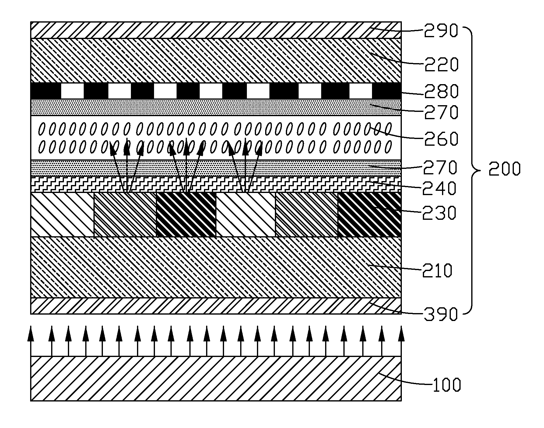
[0033]Please refer to FIG. 3, which is a sectional diagram of a liquid crystal display according to the present invention. The liquid crystal comprises a backlight module 1, and a liquid crystal panel 2 positioned on the backlight module 1.
[0034]Specifically, the liquid crystal panel 2 comprises an array substrate, an upper substrate positioned above the array substrate, an upper polarizer 29 on the upper substrate, and a liquid crystal layer 26 positioned between the array substrate and the upper substrate.
[0035]Specifically, the array substrate comprises a first glass substrate 20, a TFT layer 21 positioned on the first glass substrate 20, the color resistor layer 23 positioned on the TFT layer 21, a pixel electrode layer 24 positioned on the color resist layer 23, the polarization layer 25 positioned on the pixel electrode layer 24 and a first alignment layer 271 positioned on the polarization layer 25; the upper substrate comprises a second glass substrate 22, a black matrix 28 ...
second embodiment
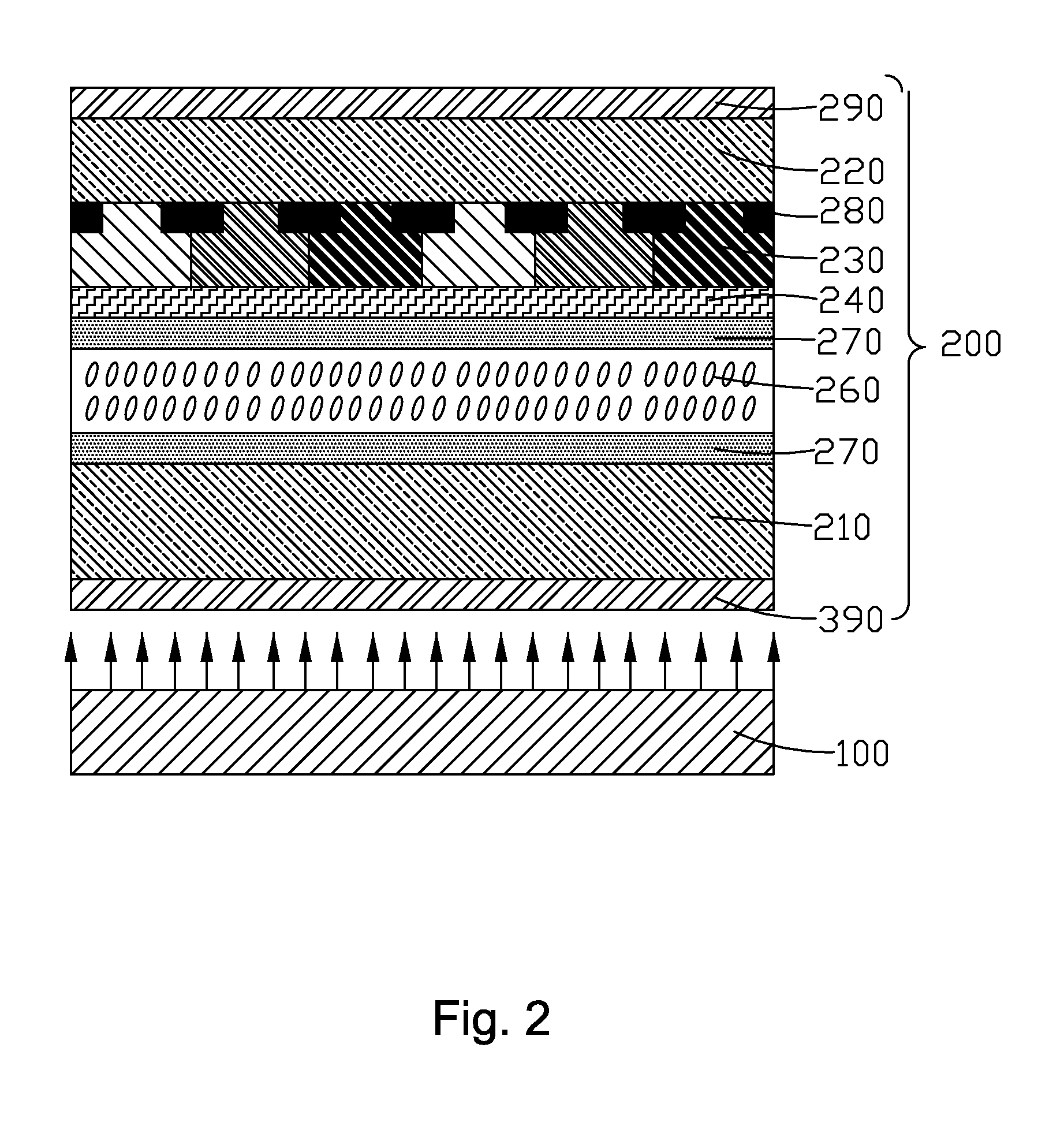
[0041]Please refer to FIG. 4, which is a sectional diagram of a liquid crystal display according to the present invention. The liquid crystal comprises a backlight module 1, and a liquid crystal panel 2 positioned on the backlight module 1.
[0042]Specifically, the liquid crystal panel 2 comprises an array substrate, a lower substrate 39 under the array substrate, a CF substrate positioned above the array substrate and a liquid crystal layer 26 positioned between the array substrate and the CF substrate.
[0043]Specifically, the array substrate comprises a first glass substrate 20, a TFT layer 21 positioned on the first glass substrate 20, a first alignment layer 271 positioned on the TFT layer 21; the CF substrate comprises a second glass substrate 22, a black matrix 28 positioned on the second glass substrate 22, the color resist layer 23 positioned on the black matrix 28, a common electrode layer 24 positioned on the color resist layer 23, the polarization layer 25 positioned on the ...
PUM
 Abstract
Description
Claims
Application Information