Ex-core nuclear instrumentation device
- Summary
- Abstract
- Description
- Claims
- Application Information
AI Technical Summary
Benefits of technology
Problems solved by technology
Method used
Image
Examples
embodiment 1
[0021
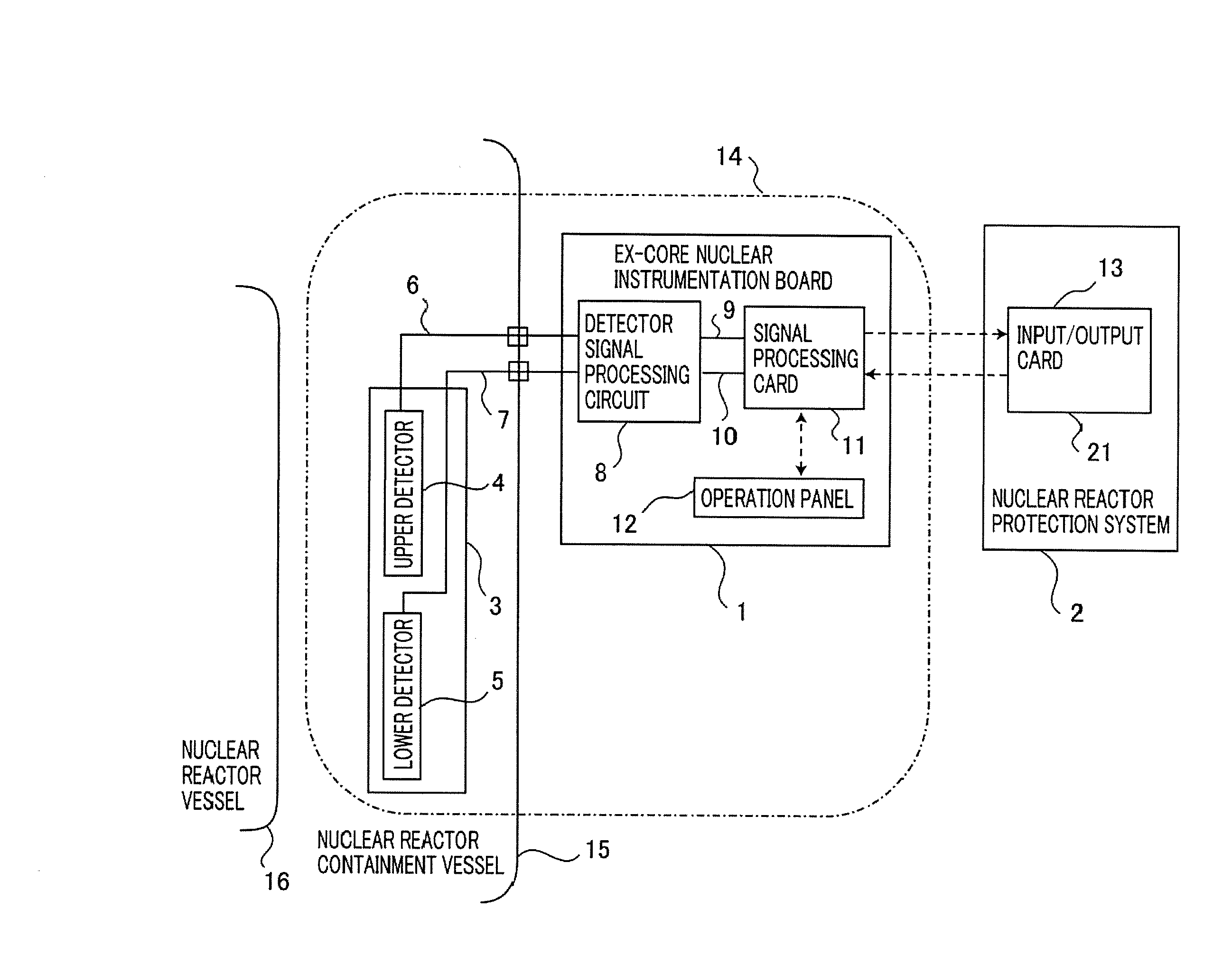
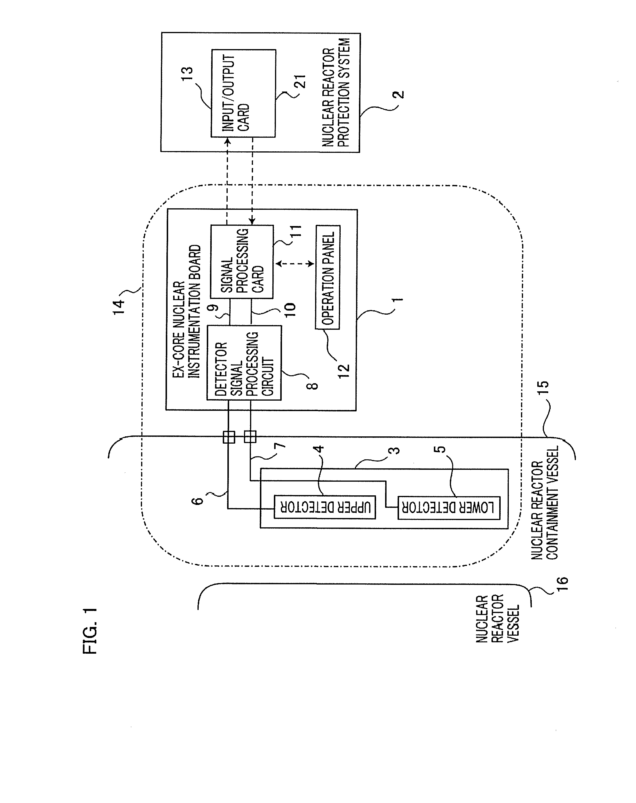
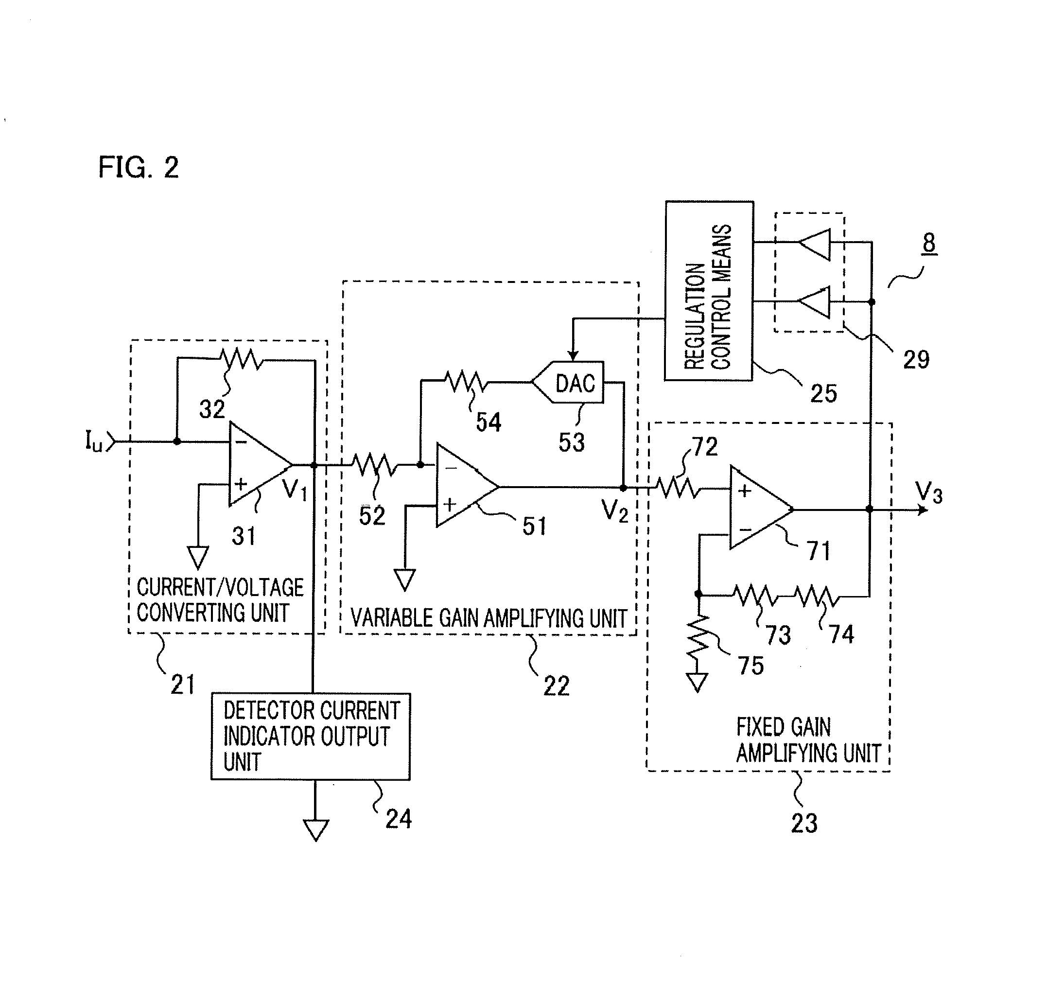
[0022]FIG. 1 is a configuration diagram illustrating a general configuration of an ex-core nuclear instrumentation device in an output region. In FIG. 1, a neutron detector 3 of an ex-core nuclear instrumentation device 14 is provided at an adjacent position of the outside of a nuclear reactor vessel 16 which is installed in a nuclear reactor containment vessel 15. The neutron detector 3 is configured by integrating an upper detector 4, which detects a neutron, which is leaked from an upper portion of the nuclear reactor vessel 16, so as to convert the neutron to a current value, and a lower detector 5, which detects a neutron, which is leaked from a lower portion of the nuclear reactor vessel 16, so as to convert the neutron to a current value. The current value, which is converted by the upper detector 4, is inputted to a detector signal processing circuit 8 in an ex-core nuclear instrumentation board 1 of the ex-core nuclear instrumentation device 14, which is generally disp...
embodiment 2
[0040
[0041]FIG. 4 is a circuit configuration diagram illustrating a detector signal processing circuit (I / E amplifier) 8 according to Embodiment 2. In Embodiment 1, a case, in which a switching control is performed by adding the current-level-responsible resistor circuit 61, which is composed of a resistor and an analog switch, to the variable gain amplifying unit 22, is described, whereas in Embodiment 2, as indicated in FIG. 4, a current-level-responsible resistor circuit 41, which is composed of a resistor and an analog switch, to a current / voltage converting unit 21 with respect to a basic circuit configuration indicated in FIG. 1. In addition, symbols 42 through 44 are resistors, and symbols 45 through 47 are analog switches. Moreover, a resistance value of the current-level-responsible resistor circuit 41 is automatically switched by a comparator 29 which is connected to a selection regulation control means 27.
[0042]In other words, when a measured current is minute and an outp...
embodiment 3
[0043
[0044]FIG. 5 is a circuit configuration diagram illustrating a detector signal processing circuit (I / E amplifier) 8 according to Embodiment 3, and two D / A converter 55 (DAC1) and D / A converter 56 (DAC2) are connected in series in such a way that the D / A converters of a variable gain amplifying unit 22 are connected as a two-stage configuration with respect to FIG. 1.
[0045]The unilateral D / A converter 55 corresponds to the current-level-responsible resistor circuit 61 according to Embodiment 1, and a resistance value is largely selected by a selection regulation control means 28 based on a comparator 29, and the other D / A converter 56 corresponds to the D / A converter 53 according to Embodiment 1, and a resistance value is mutely regulated by the selection regulation control means 28 based on the comparator 29. Therefore, a width of a gain of the variable gain amplifying unit 22, in other words, a width of a gain of the detector signal processing circuit 8 can be automatically va...
PUM
 Abstract
Description
Claims
Application Information


