Scanning probe lithography methods
a scanning probe and nanofabrication technology, applied in the direction of electrical equipment, instruments, electric discharge tubes, etc., can solve the problem of limited fabrication speed of several nanometers per second
- Summary
- Abstract
- Description
- Claims
- Application Information
AI Technical Summary
Benefits of technology
Problems solved by technology
Method used
Image

Examples
example 1
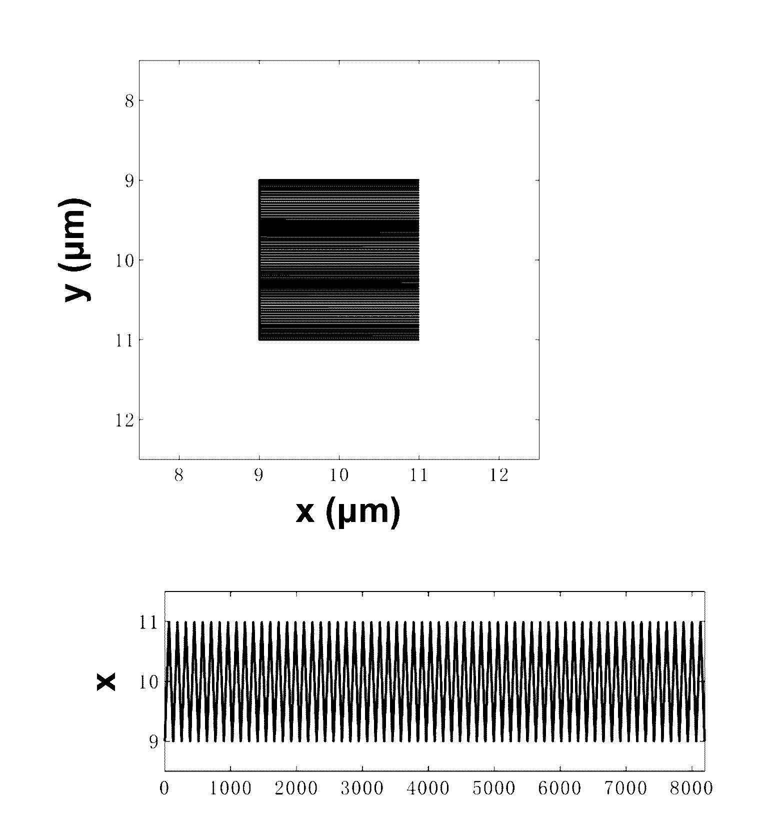
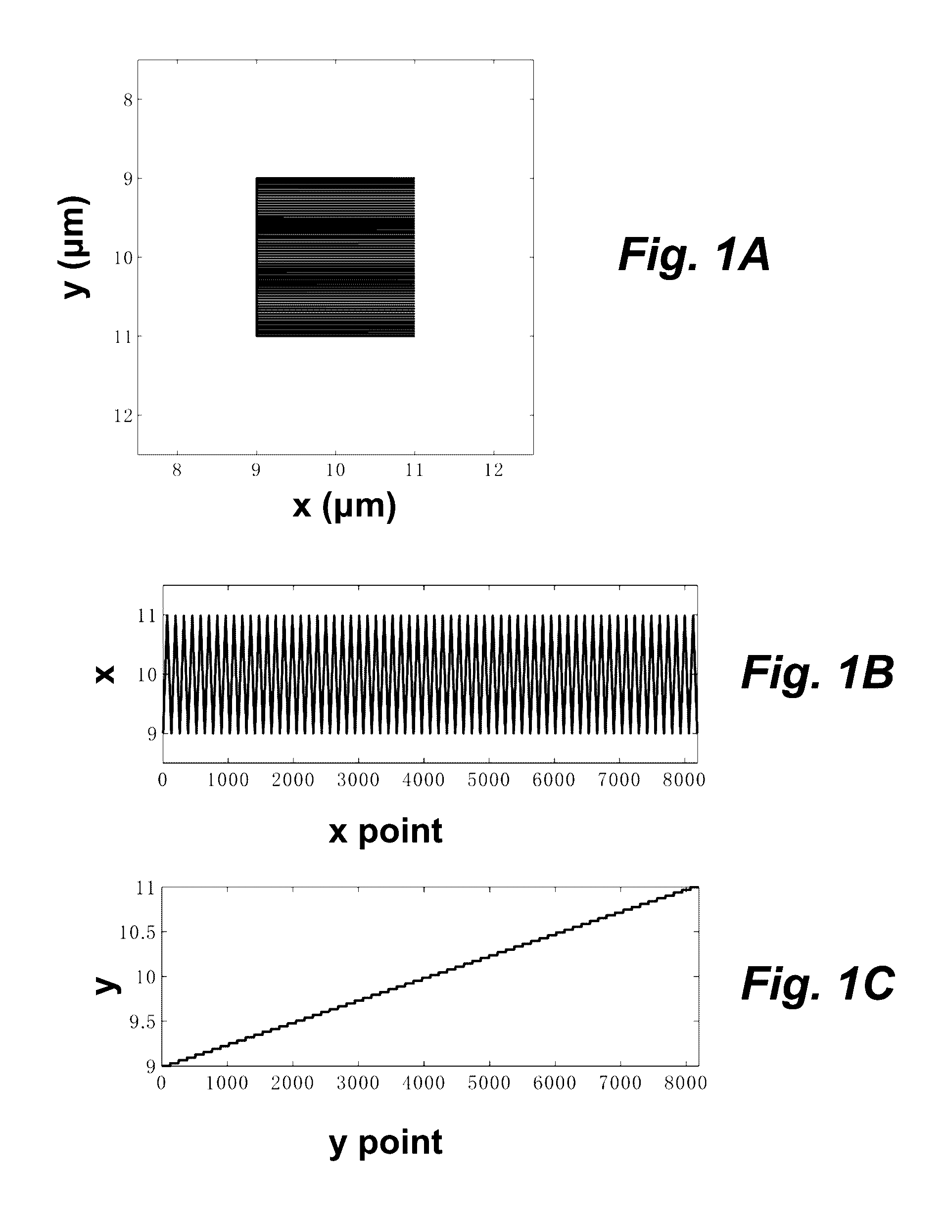
[0056]SPN surface modifications and characterization were carried out under ambient conditions by using a Veeco Dimension V AFM with Nanoscope V Controller. Standard tapping mode silicon cantilevers (RTESP, Bruker, nominal spring constant k=40 N / m, resonance frequency f0=350 kHz) were used to effect mechanical scratching. Before the experiments, the deflection sensitivity and the spring constant of the cantilevers were calibrated by using the force distance curves and the thermal tune method (Levy et al., Nanotechnology 13 (1), 33 (2002)), respectively. For sample preparations, a surface treatment was performed to form a monolayer of C18 chains on a clean Si / SiO2 substrate for scratching fabrications. The thickness of the film was ˜5 nm as measured by AFM height imaging on the edges of the film. The average surface roughness measured was ˜2.5 nm. After scratching, the topography of the modified surfaces can be characterized by tapping mode AFM. For tip triboelectrification experimen...
example 2
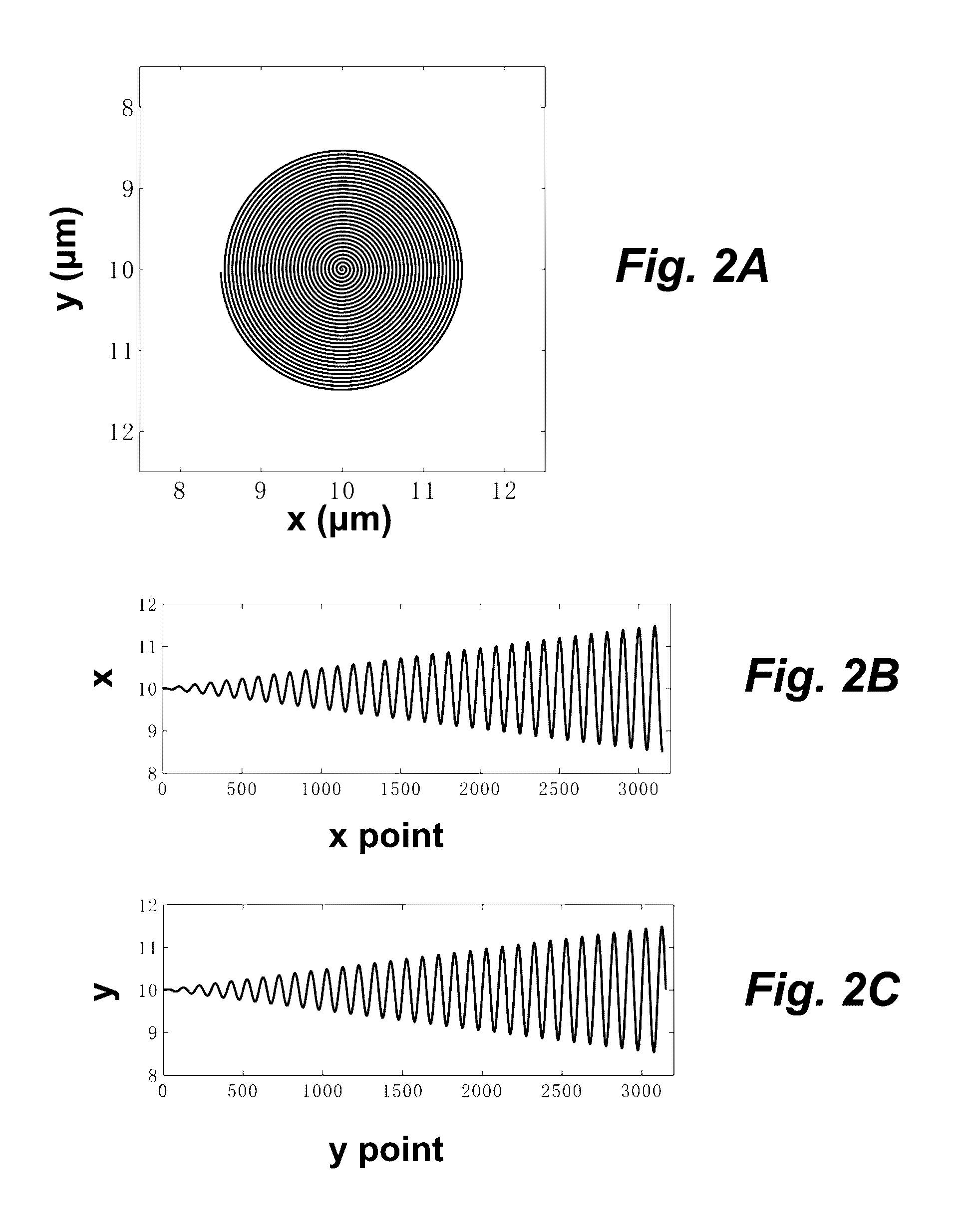
[0059]As another application, a tip-based triboelectrification fabrication with Lissajous patterns was conducted. By using a silicon AFM tip to contact a silicon dioxide surface, negative charges are generated and accumulated on the rubbed surface during scanning. The surface potential generated by the charges are characterized by SKPM. In experiments, for in situ modification and characterization, a worn-out conductive AFM tip was used. Contacting the surface with silicon tip and sensing the electrostatic field can be simultaneously satisfied. For charge generation in contact mode, the trajectory used is the same as in the FIG. 3C. The cantilever deflection sensitivity (˜32.10 mn / V), the setpoint value (˜0.2 V), and the force constant (˜1.63 N / m) were calibrated before the fabrications. The normal force (˜10 nN) was evaluated with Hook's law by multiplying these parameters. Two cycles of the Lissajous trajectory were performed in charge generation mode, such that the squared area w...
embodiment 1
[0061]A method of creating a pattern with a scanning probe nanofabrication device or an ion beam micromachining device comprising moving, with an enclosed sinusoidal trajectory, a substrate upon which the pattern will be formed relative to (a) a tip of the scanning probe nanofabrication device or (b) the ion beam.
PUM
 Abstract
Description
Claims
Application Information