Eureka AIR delivers breakthrough ideas for toughest innovation challenges, trusted by R&D personnel around the world.

Semiconductor device and manufacturing method thereof

Active Publication Date: 2017-02-23
RENESAS ELECTRONICS CORP
View PDF5 Cites 1 Cited by
  • Summary
  • Abstract
  • Description
  • Claims
  • Application Information

AI Technical Summary

Benefits of technology

The patent text describes a way to make semiconductor devices that have better performance and reliability. This is done by improving the design of the part of the device called the trench gate IGBT.

Problems solved by technology

However, there is the fear that, when an emitter wire is coupled to the emitter electrode, stress in the emitter wire may be concentrated in an acute angle portion at the end of the emitter coupling portion, whereby a crack may be caused.
Additionally, because concavities and convexities are formed in the surface of the emitter electrode, there is the problem, that the adhesiveness between the emitter wire and the emitter electrode is deteriorated.

Method used


Image

  • Semiconductor device and manufacturing method thereof
  • Semiconductor device and manufacturing method thereof
  • Semiconductor device and manufacturing method thereof

Examples


embodiment

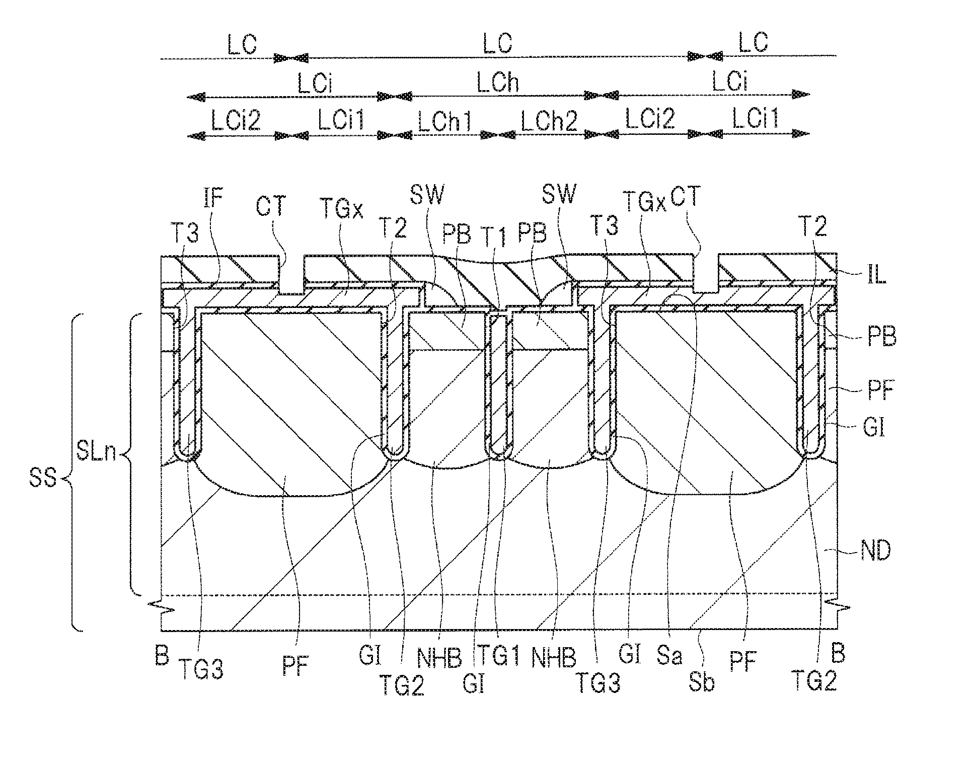
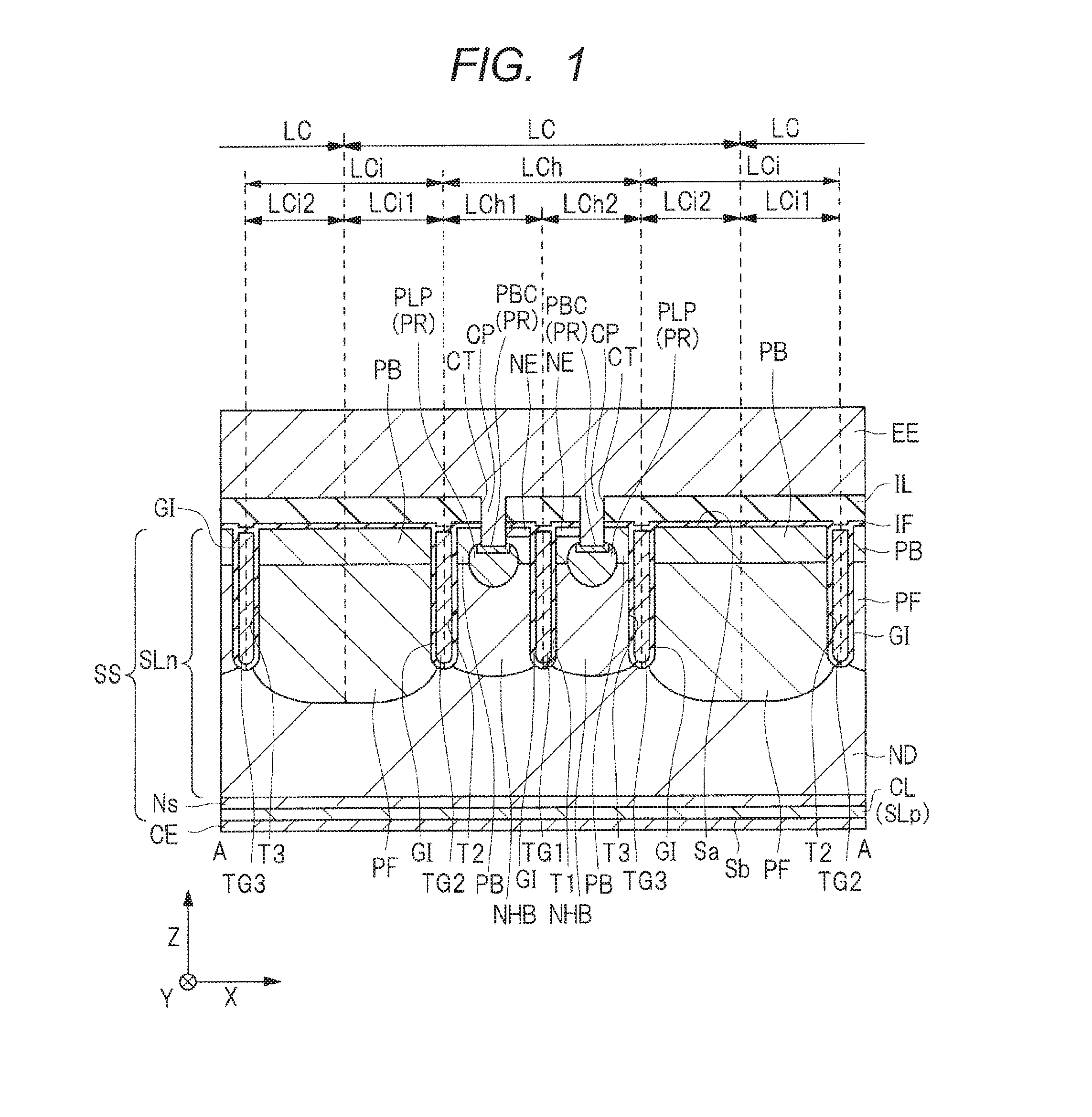
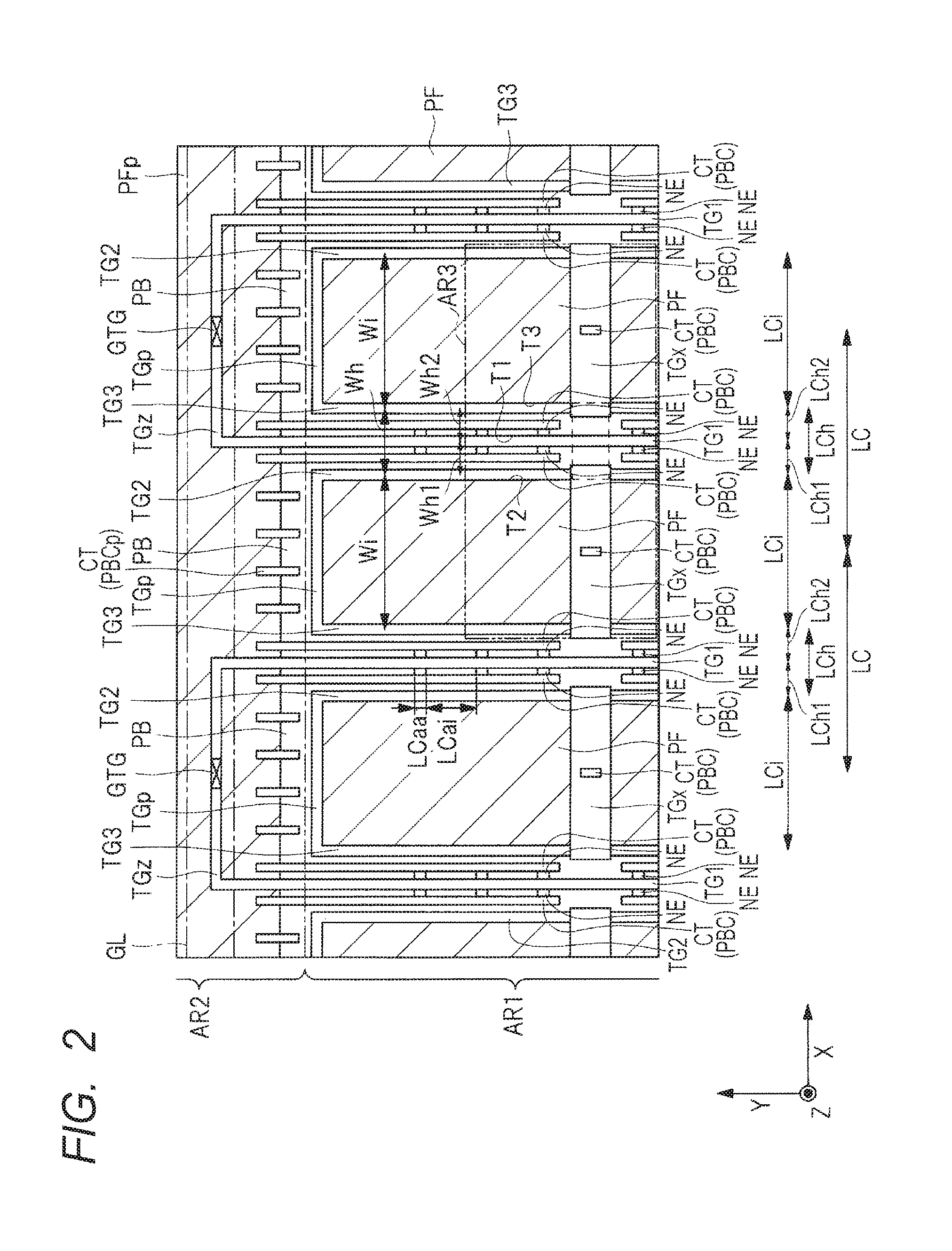
[0055]Hereinafter, a semiconductor device according to the present embodiment will be described in detail with reference to drawings. The semiconductor device according to the embodiment is an IE-type trench gate IGBT. The semiconductor device exhibits an IE effect in which, when the IGBT is in an ON state, discharge of holes toward the side of an emitter electrode (surface side) is restricted, whereby the concentration of the holes stored in a drift region can be increased, and hence the semiconductor device is referred to as an IE type. Further, of three trench gate electrodes arrayed to be spaced apart from each other in the semiconductor device according to the embodiment, the trench gate electrode (TG1) arranged in the center is electrically coupled to a gate electrode, and each of the two trench gate electrodes (TG2, TG3) arranged at both the ends is electrically coupled to an emitter electrode, and hence the semiconductor device is also referred to as an EGE type (Emitter-Gat...


PUM


Abstract

The surface of an interlayer insulating film formed over an emitter coupling portion and the surface of an emitter electrode formed over the interlayer insulating film are caused to have a gentle shape, in particular, at the end of the emitter coupling portion, by forming the emitter coupling portion over a main surface of a semiconductor substrate and integrally with trench gate electrodes in order to form a spacer over the sidewall of the emitter coupling portion. Thereby, stress is dispersed, not concentrated in an acute angle portion of the emitter coupling portion when an emitter wire is coupled to the emitter electrode (emitter pad), and hence occurrence of a crack can be suppressed. Further, by forming the spacer, the concavities and convexities to be formed in the surface of the emitter electrode can be reduced, whereby the adhesiveness between the emitter electrode and the emitter wire can be improved.

Description

CROSS-REFERENCE TO RELATED APPLICATIONS[0001]The disclosure of Japanese Patent Application No. 2015-162718 filed on Aug. 20, 2015 including the specification, drawings and abstract is incorporated herein by reference in its entirety.BACKGROUND[0002]The present invention relates to a semiconductor device and a manufacturing method thereof, and can be preferably used in a semiconductor device including, for example, an IE (Injection Enhancement) type trench gate IGBT (Insulated Gate Bipolar Transistor).[0003]For example, Japanese Unexamined Patent Application Publication No. 2013-140885 (Patent Document 1) discloses an IE-type trench gate IGBT basically formed by a first linear unit cell region having a linear active cell region, a second linear unit cell region having a linear hole collector cell region, and a linear inactive cell region between them.RELATED ART DOCUMENTPatent Document[0004][Patent Document 1] Japanese Unexamined Patent Application Publication No. 2013-140885SUMMARY[...

Claims


Application Information

Patent Timeline
IPC IPC(8): H01L29/739H01L21/768H01L23/535H01L29/10H01L29/66
CPCH01L29/7397H01L29/1004H01L21/76895H01L29/66348H01L23/535H01L29/1095H01L29/0619H01L29/0696H01L29/407H01L29/402H01L29/41725H01L29/4236H01L21/32155H01L29/66325H01L29/6656H01L29/7393H01L29/7843
Inventor MATSUURA, HITOSHI
Owner RENESAS ELECTRONICS CORP
Why Eureka
Eureka Blog
Learn More