

Wafer structure, fabrication method, and spray apparatus
a technology of wafers and spraying devices, applied in the direction of electrical equipment, semiconductor devices, semiconductor/solid-state device details, etc., can solve the problems of easy peeling of the glue layer formed by existing techniques, difficult adhesion of metal materials used for forming interconnect structures to semiconductor materials of device structures, and inability to provide enough surface area of a wafer, etc., to reduce the stress between the wafer and the glue layer, the effect of reducing the mismatch of latti
- Summary
- Abstract
- Description
- Claims
- Application Information
AI Technical Summary
Benefits of technology
Problems solved by technology
Method used
Image

Examples
Embodiment Construction
[0016]Reference will now be made in detail to exemplary embodiments of the invention, which are illustrated in the accompanying drawings. Wherever possible, the same reference numbers will be used throughout the drawings to refer to the same or like parts.
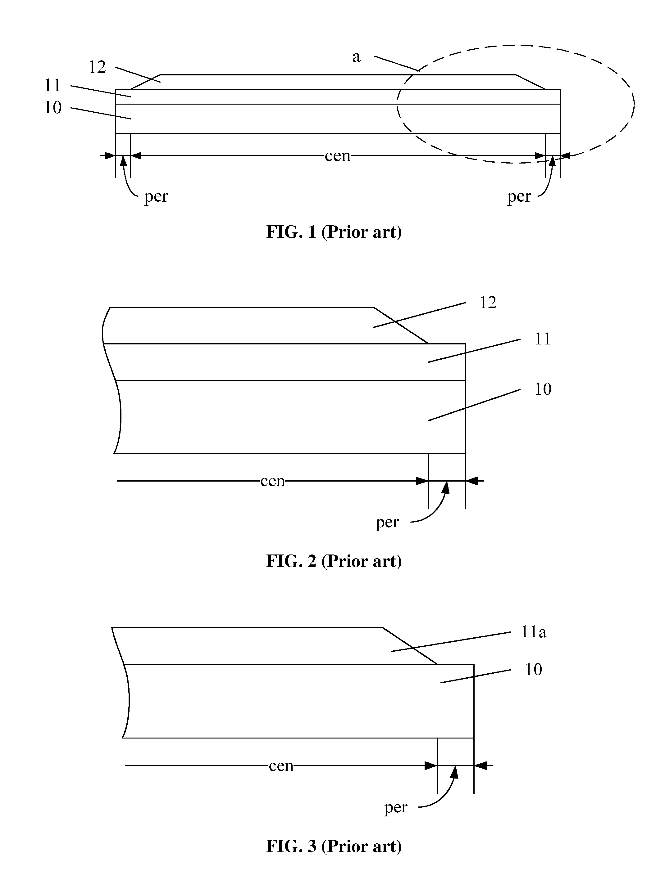
[0017]FIGS. 1-4 illustrate structures corresponding to certain stages of an existing fabrication process of a glue layer or an adhesion layer. The glue layer is used as a part of the interconnect structure.
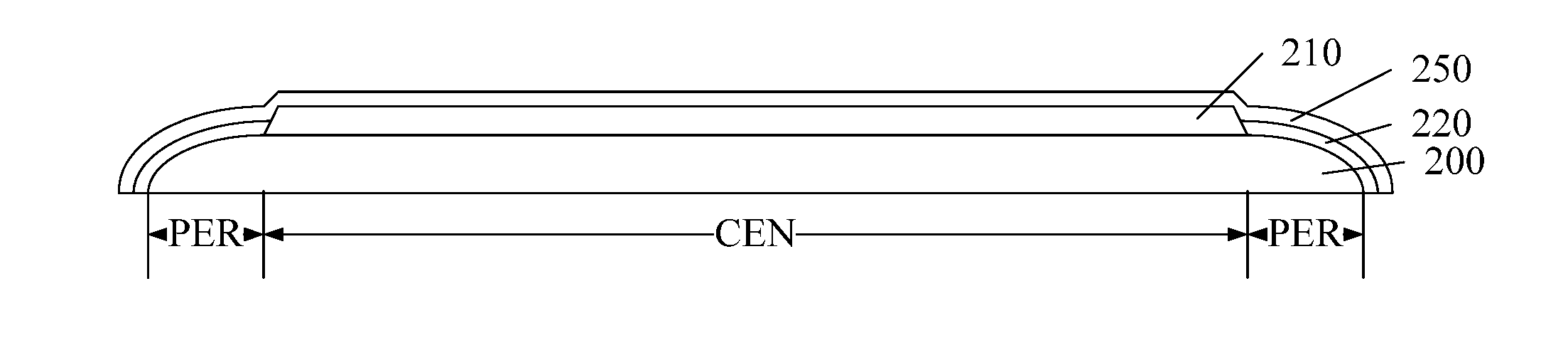
[0018]As shown in FIGS. 1-2 (FIG. 2 is a zoom-in image of the position “a” illustrated in FIG. 1), the fabrication process includes providing a wafer 10. The wafer 10 has a central region “cen” and a peripheral region “per”. An interlayer dielectric layer 11 and a mask layer 12 are sequentially formed on the surface of the wafer 10.
[0019]During the process for forming the interconnect structure by etching the inter layer dielectric layer 11, a sidewall collapsing phenomenon may happen in the peripheral region “per’ of the mask la...
PUM
 Abstract
Description
Claims
Application Information