Semiconductor device and method of manufacturing the same

a technology of semiconductor devices and semiconductor layers, applied in the direction of semiconductor devices, basic electric elements, electrical equipment, etc., can solve the problem of lateral notch in the gate oxide layer

Active Publication Date: 2017-03-02
RENESAS ELECTRONICS CORP
View PDF0 Cites 16 Cited by
  • Summary
  • Abstract
  • Description
  • Claims
  • Application Information

AI Technical Summary

Benefits of technology

[0012]According to the one embodiment described above, a semiconductor device in which the collapse of a stacked structure of a floating gate and a control gate can be prevented if megasonic cleaning is applied, and a method of manufacturing the same can be realized.

Problems solved by technology

As a result, the gate oxide layer below the floating gate erodes in a lateral direction, causing a lateral notch to occur in the gate oxide layer.

Method used


Image

  • Semiconductor device and method of manufacturing the same
  • Semiconductor device and method of manufacturing the same
  • Semiconductor device and method of manufacturing the same

Examples


first embodiment

[0048]First, each region disposed on a main surface of a semiconductor substrate in a semiconductor device of this embodiment is described with reference to FIG. 1.

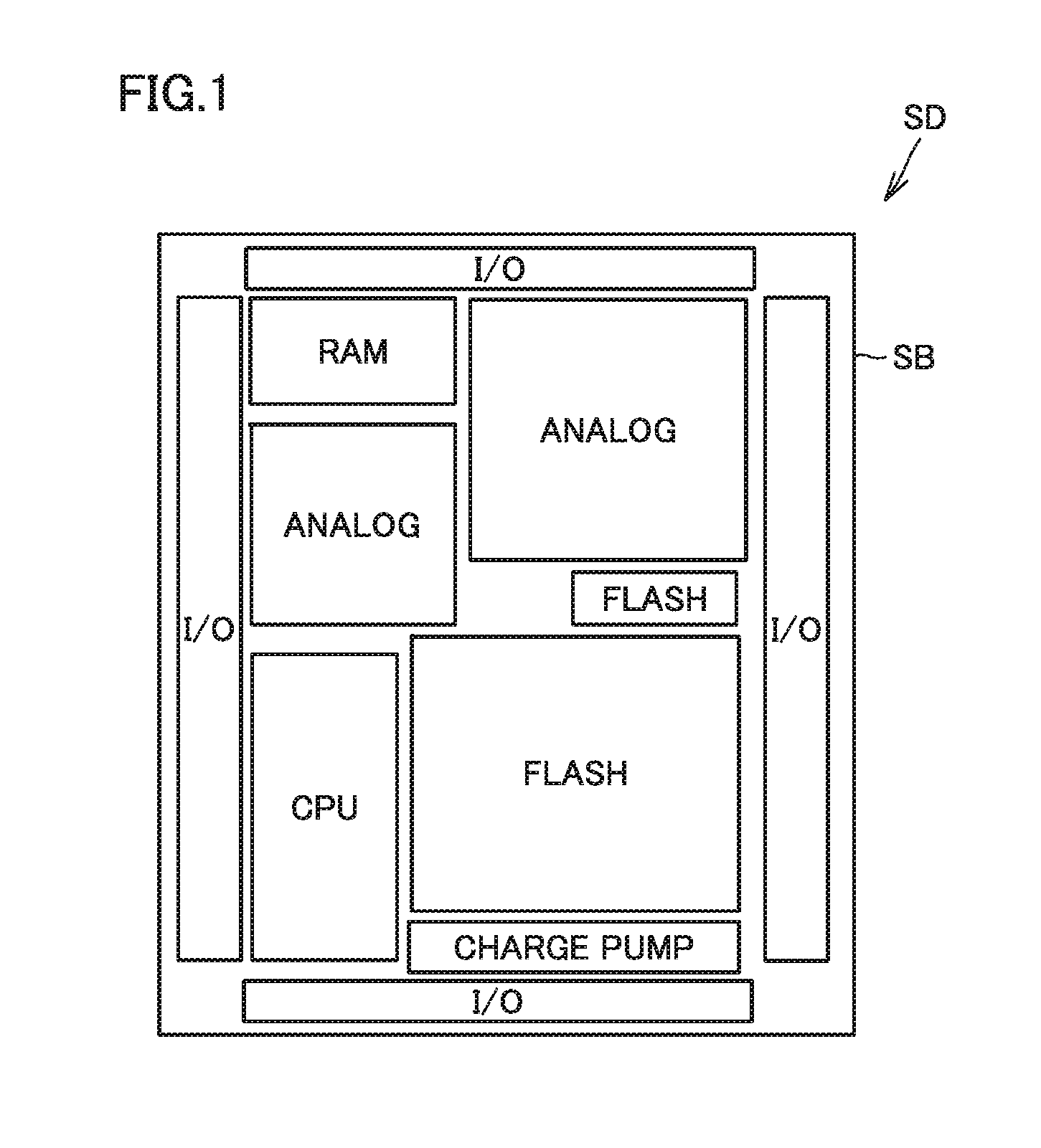
[0049]As shown in FIG. 1, a semiconductor device SD in this embodiment is in the form of a chip, for example. Alternatively, semiconductor device SD in this embodiment may be in the form of a wafer, or in the form of a resin-sealed package.

[0050]Semiconductor device SD in this embodiment mainly has, on the surface of a semiconductor substrate SB, an I / O (Input / Output) region, an ANALOG region, a RAM (Random Access Memory) region, a CPU (Central Processing Unit) region, a charge pump region, and a flash memory region, for example.

[0051]In the flash memory region, a plurality of nonvolatile flash memory cells are arranged in columns.

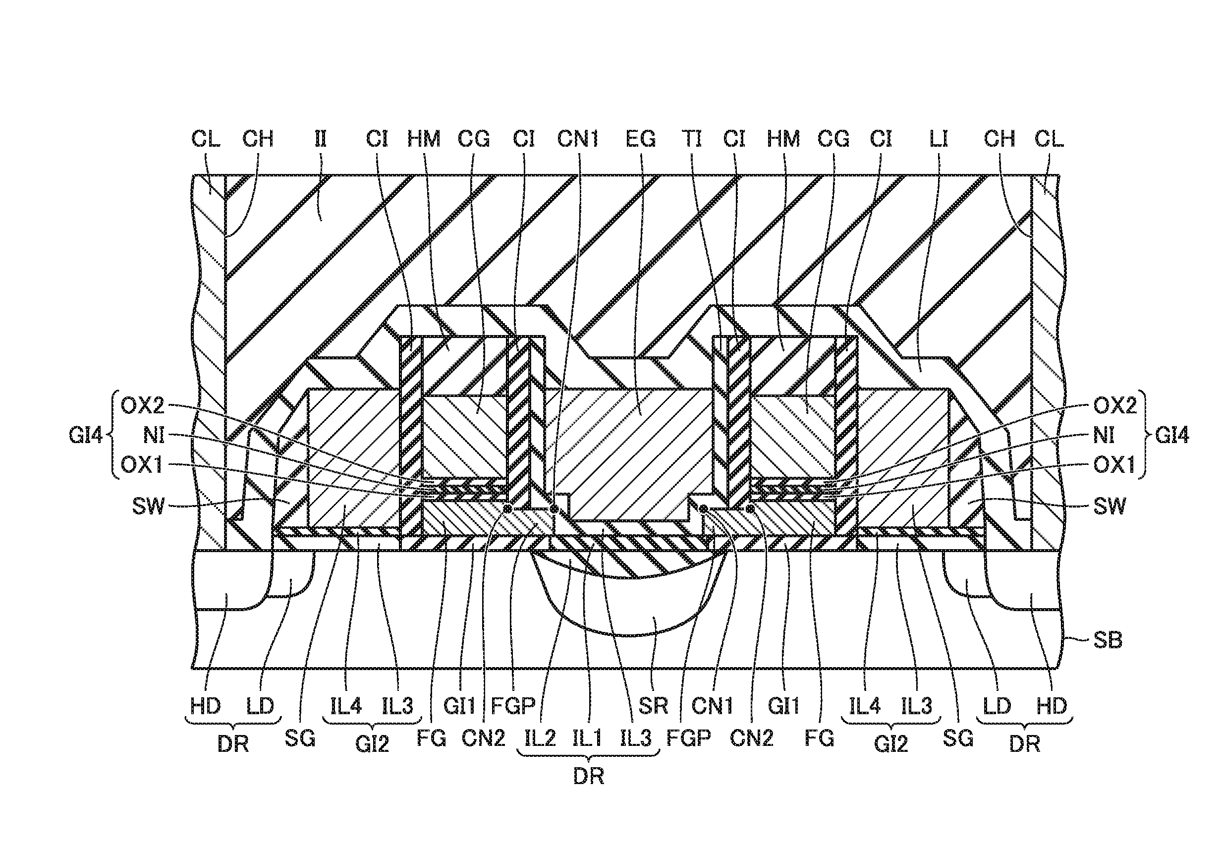
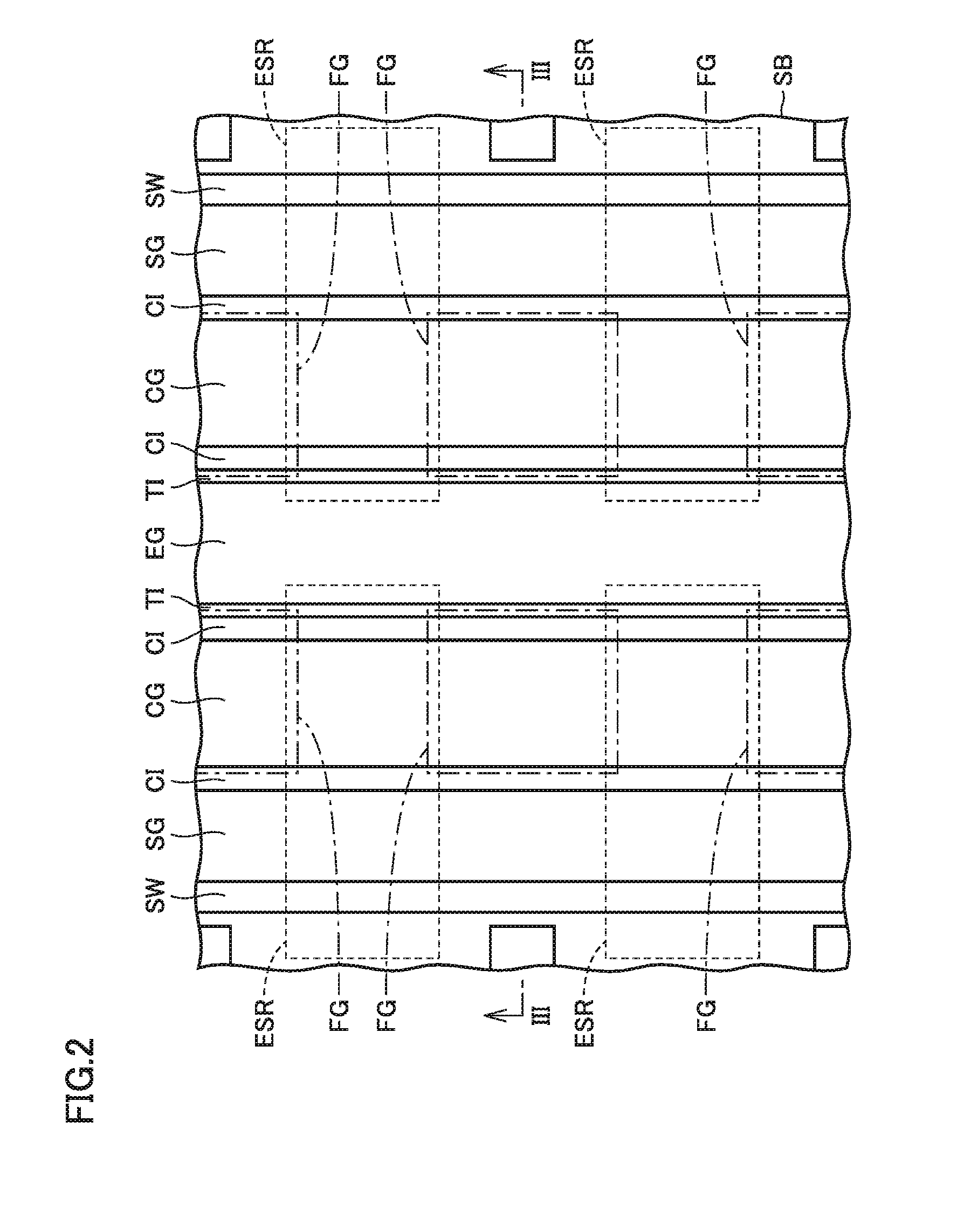
[0052]Next, the configuration of each of the nonvolatile flash memory cells in this embodiment is described with reference to FIGS. 2 and 3.

[0053]As mainly shown in FIG. 2, the nonvolatile flash...

second embodiment

[0128]A method of manufacturing a semiconductor device of this embodiment includes similar steps to those of the first embodiment shown in FIGS. 4 to 13. In this embodiment, after insulating film SL1 (first sidewall insulating film) is removed as shown in FIGS. 12 to 13, nitrogen introduced portion IL1 (first nitrogen introduced portion) is removed by anisotropic etching until the main surface of semiconductor substrate SB is exposed as shown in FIG. 24. Then, the manufacturing method of this embodiment includes similar steps to those of the first embodiment shown in FIGS. 14 to 22. A semiconductor device shown in FIG. 25 is thus manufactured.

[0129]As shown in FIG. 25, the semiconductor device manufactured according to this embodiment does not have nitrogen introduced portion IL1 between erase gate EG and semiconductor substrate SB. Accordingly, only insulating films IL2 and IL3 made of silicon oxide, for example, exist between erase gate EG and semiconductor substrate SB.

[0130]The ...

third embodiment

[0132]A method of manufacturing a semiconductor device of this embodiment includes similar steps to those of the first embodiment shown in FIGS. 4 to 14. After source region SR is formed in FIG. 14, in this embodiment, nitrogen is introduced into insulating film SL2 as shown in FIG. 26.

[0133]As the conditions for the nitrogen introduction, average projection range Rp is between 50 nm and 90 nm, and implantation energy is between 8 keV and 15 keV, for example. As the conditions for the nitrogen implantation described above, an implantation angle is 0 degree, and a dose amount is between 1×10¹⁵ atoms / cm2 and 5×10¹⁵ atoms / cm2, for example.

[0134]As a result, a nitrogen introduced portion NL1 (partial nitrogen introduced portion) and a nitrogen introduced portion NL2 are formed in a portion of insulating film SL2. Nitrogen introduced portion NL1 is formed to be located on the upper surface of nitrogen introduced portion IL1, and also to be located on the side surface of lateral protrusio...


PUM


Abstract

An insulating film made of the same material as that of a gate insulating film is formed so as to cover one sidewall of a control gate on a conducting film for floating gate. By selectively removing the conducting film for floating gate with the insulating film as a mask, a floating gate is formed from the conducting film for floating gate, and a portion of the gate insulating film is exposed at the floating gate. A nitrogen introduced portion is formed by introducing nitrogen into the exposed portion of the gate insulating film. Then, the insulating film is removed to expose an upper surface of a lateral protrusion of the floating gate. An erase gate is formed so as to face the upper surface and a side surface of the lateral protrusion.

Description

[0001]This nonprovisional application is based on Japanese Patent Application No. 2015-164789 filed on Aug. 24, 2015, with the Japan Patent Office, the entire contents of which are hereby incorporated by reference.BACKGROUND OF THE INVENTION[0002]Field of the Invention[0003]The present invention relates to semiconductor devices and methods of manufacturing the same.[0004]Description of the Background Art[0005]Examples of nonvolatile flash memories include a split gate memory having a floating gate, a control gate, an erase gate and a select gate. Such a nonvolatile flash memory is disclosed, for example, in Japanese Patent Laying-Open No. 2009-44164.[0006]In this publication, after the control gate is patterned, a spacer oxide layer is formed on sidewalls of the control gate. With this spacer oxide layer as a mask, the floating gate below the control gate and the spacer oxide layer is patterned. The spacer oxide layer is then removed.[0007]In the manufacturing method of the above pu...

Claims


Application Information

Patent Timeline
Patent Type & Authority Applications(United States)
IPC IPC(8): H01L27/115H01L29/423
CPCH01L29/42328H01L27/11521H01L29/40114H10B41/35H10B41/30
Inventor KODAMA, SATOSHIHASEGAWA, EIJI
Owner RENESAS ELECTRONICS CORP
Why Eureka
Try Eureka